8A3xxxx 144BGA EVK User Manual
© 2019 Integrated Device Technology, Inc.
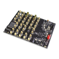
• VCCO voltage selection jumpers – Each output voltage can be individually supplied with 1.8V, 2.5V, or 3.3V. These jumpers are used to
select the voltage for the output voltages.
• Reset button – A small button is used to reset the board.
• OSCI Input connector – An SMA connector, J45, can optionally supply a clock signal to overdrive the crystal.
• OCXO/TCXO reference – An SMA connector, J46, can supply a local OCXO/TCXO reference as an optional reference for System DPLL.
• Crystal – A crystal of various frequencies must be present for board operations. A 3225 footprint is provided for SMT crystals. For easy
plug-in of a canned crystal, two through holes are also available.
• EEPROM – An SO-8 socket is provided to hold an EEPROM device of compatible package. EEROM is used to store firmware and
customer configuration data, if needed.
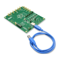
1.2 Board Power Supply
The board uses a single +5V supply for its power supplies. When running the board, set the bench power supply at 5V/2A. The red jack (J1) is
positive; the black jack (J2) is the ground.
Multiple LDOs are used to generate 3.3V, 2.5V, and 1.8V from the +5V supply.
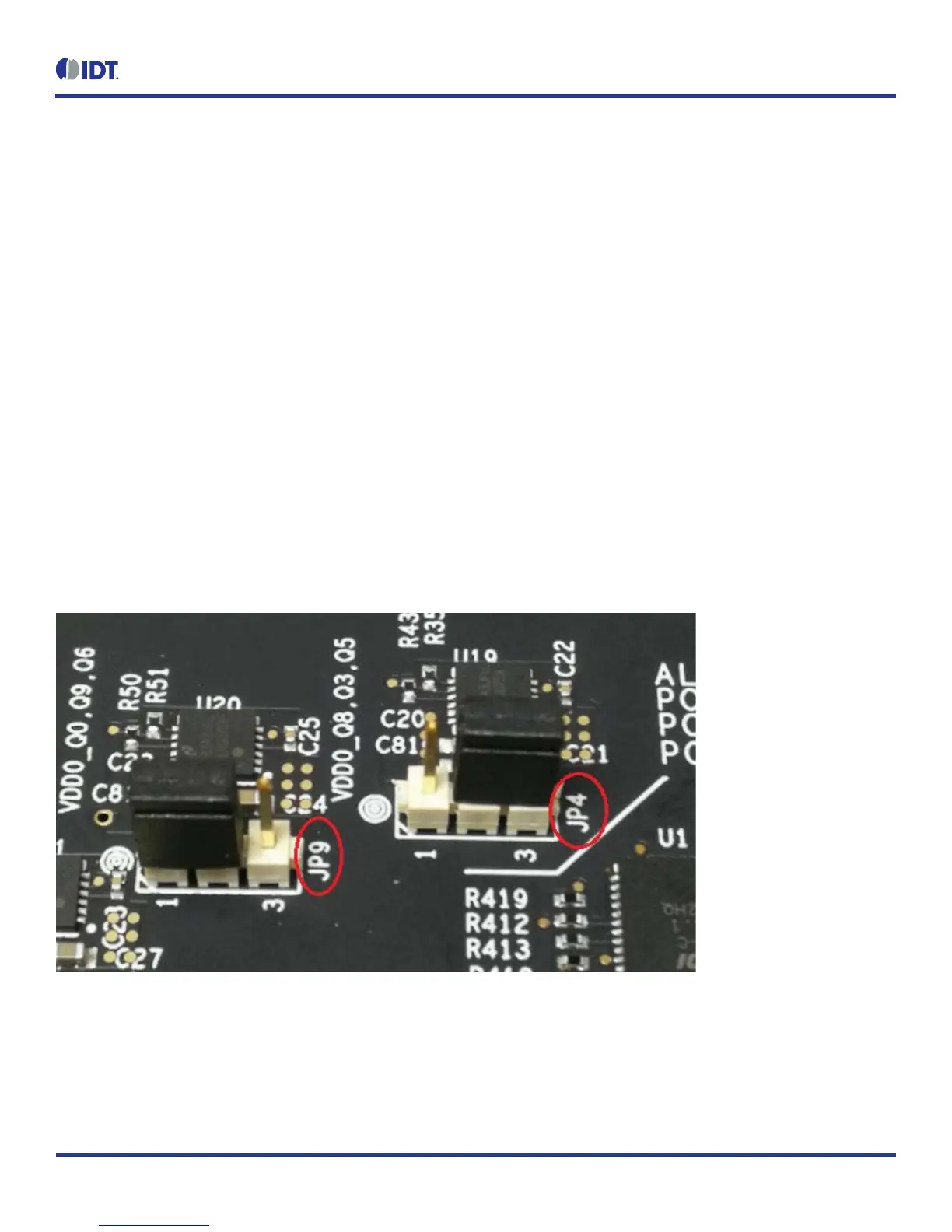
1.3 Voltage Selection Jumpers
There are nine headers/jumpers to select different voltages for different functional blocks of the chip. Each head is labeled pin 1 and pin 3 –
jumping pin 1 and pin 2 will select 3.3V; jumping pin 2 and pin 3 will select 2.5V; no jumper will have 1.8V.
Please see the following example for JP4 and JP9 – JP4 will select 2.5V; JP9 will select 3.3V.
Figure 2. Example of Voltage Jumpers
 Loading...