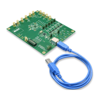
8A3xxxx 144BGA EVK User Manual
© 2019 Integrated Device Technology, Inc.
The following list shows which head/jumper is used to select what voltage:
• JP1 – VDDD
• JP2 – VDDA
• JP3 – VCC_GPIO_DC
• JP4 – VDDO_Q8_3_5
• JP5 – VDDO_Q2_4_11
• JP6 – VDDO_1_10_7
• JP7 – VDD_CLK0
• JP8 – VDD_CLK1
• JP9 – VDDO_Q0_9_6
Important Equipment Warning: VDD_FOD voltage is selected by resistors R908 and R909. In order to prevent
damage to the device, both R908 and R909 should not be stuffed, in which case VDD_FOD = 1.8V.
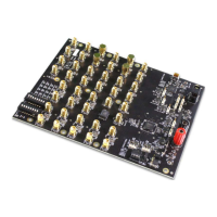
1.4 GPIO Switches, LEDs, and Test Points
Two 8-bit dip switches sets the logic levels for 16 GPIOs. The following table shows the GPIO levels for each setting and the corresponding
LED state.
Table 1. GPIO Settings
Dip Switch Position GPIO Logic Level LED
Left Low On
Center
High if GPIO is configured as Input
High or Low according to the GPIO output setting
High if GPIO is configured as Input
High or Low according to the GPIO output setting
Right High Off
Please see the picture and labels in Figure 3.
When the GPIOs are configured as outputs (such as User-Controlled or LOL indicator), the dip switch for the corresponding GPIO should be
placed in the center position. The LED will indicate the state of the GPIO.
 Loading...