8A3xxxx 144BGA EVK User Manual
© 2019 Integrated Device Technology, Inc.
1. Usage Guide
1.1 Board Overview
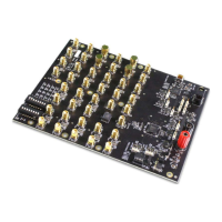
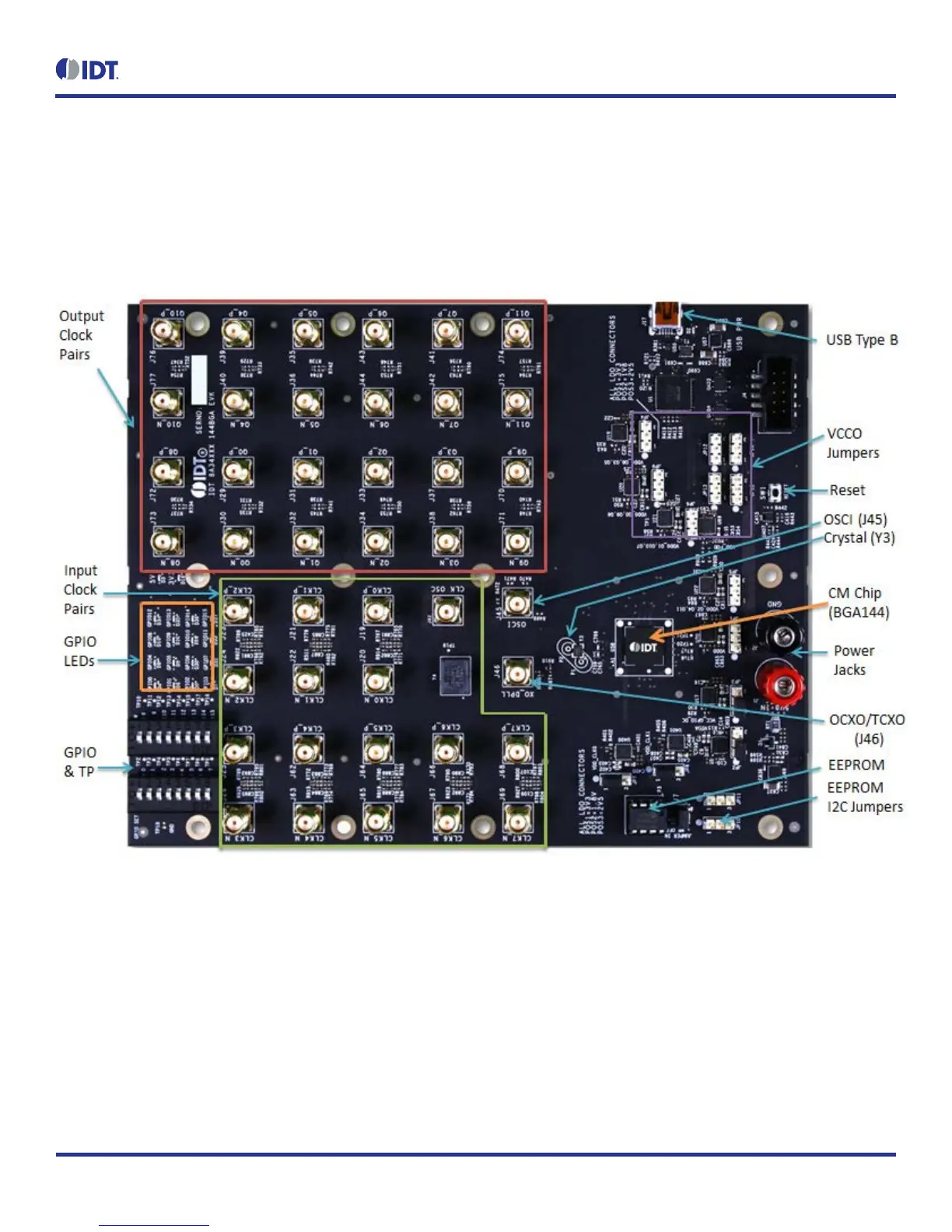
The following diagram identifies various components of the board: input and output SMA connectors, power supply jacks, and some jumper
settings necessary for the board operations.
Figure 1. Overview of 144BGA ClockMatrix Evaluation Board
Detailed descriptions of the board are as follows.
• Input SMA Connectors – There are eight differential inputs labeled CLK0/nCLK0–CLK7/nCLK7. Each input clock can be configured
differentially (LVDS, PECL 2.5V, and PECL 3.3V) or in single-ended format (CMOS).
• Output SMA Connectors – There are 12 outputs labeled as Q0/nQ0–Q11/nQ11. Each output clock can be configured differentially (LVDS,
LVPECL, or user-defined amplitude), or in single-ended format (LVCMOS – in-phase or out-of-phase)
• GPIO switch, LEDs, and test points – There are 16 GPIOs available. Each GPIO can be set a “low” or “high” level (if input) or displayed
with an LED (if output). Some GPIOs are used to set the chip in a certain working condition on power-up. For more information, see GPIO
Switches, LEDs, and Test Points.
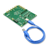
• USB connector – A USB mini-connector connects the evaluation board to a PC for GUI communications. No power is drawn from the USB
connector other than to power the FTDI USB chip.
 Loading...