Q770 Technical Service Manual
--45--
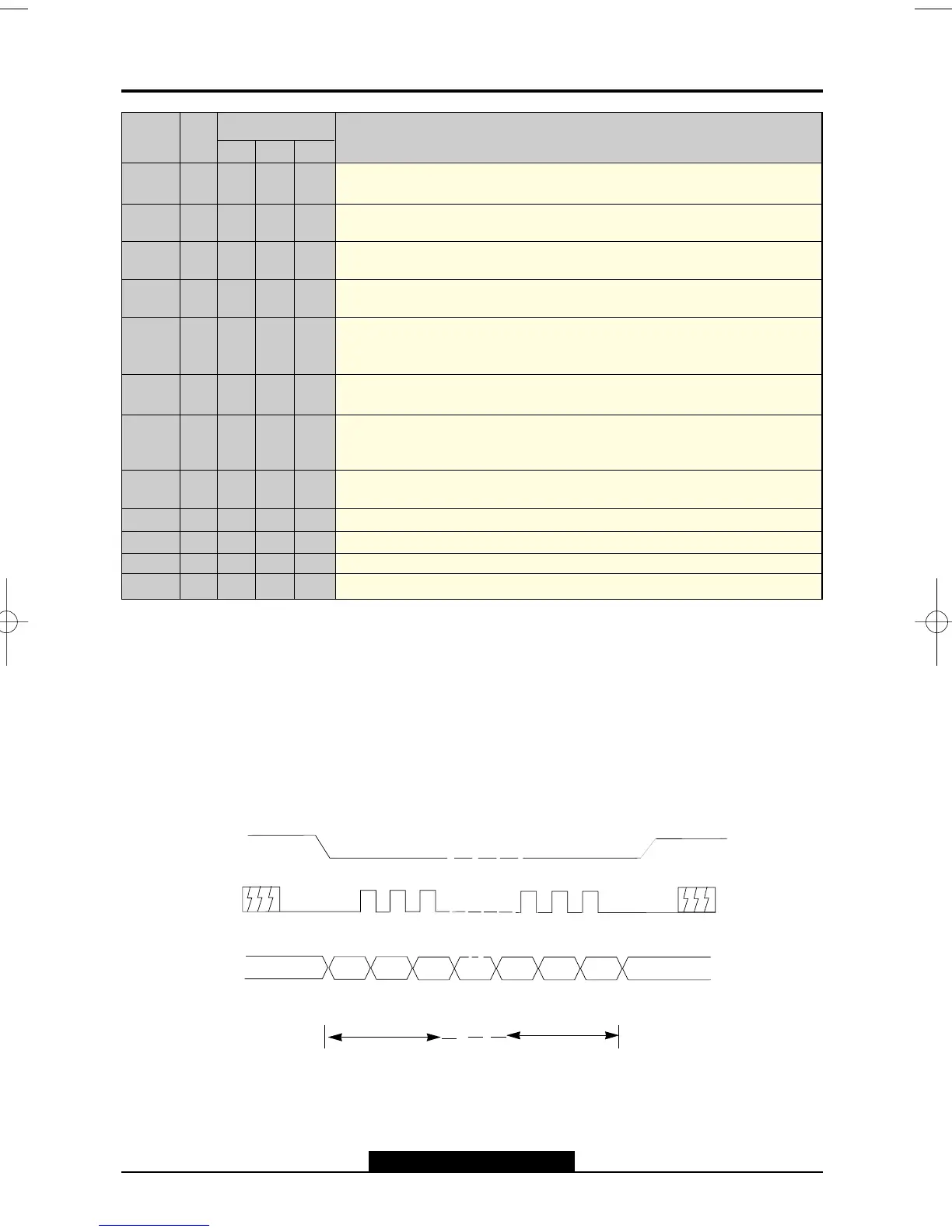
first byte last byte
FIGURE 1. Data Transmission Protocol(SPI)
Name
PWM4
PWM5
PWM6
PWM7
VDD
VFLB
HTONE/
PWMCK
FBKG
BOUT
GOUT
ROUT
VSS
I/O
O
O
O
O
-
I
O
O
O
O
O
O
PIN NO.
N16 N20 N24
- - 13
- - 14
- 11 15
- 12 16
9 13 17
10 14 18
11 15 19
12 16 20
13 17 21
14 18 22
15 19 23
16 20 24
Descriptions
Open-Drain PWM D/A converter 4. The output pulse width is program-
mable by the register of Row 15, Column 27.
Open-Drain PWM D/A converter 5. The output pulse width is program-
mable by the register of Row 15, Column 28.
Open-Drain PWM D/A converter 6. The output pulse width is program-
mable by the register of Row 15, Column 29.
Open-Drain PWM D/A converter 7. The output pulse width is program-
mable by the register of Row 15, Column 30.
Digital power supply. Positive 5V DC supply for internal digital circuitry
and a 0.1uF decoupling capacitor should be connected across to VDD and
VSS.
Vertical input. This pin is used to input the vertical synchronizing signal.
it is leading triggered and has an internal pull-up resistor.
Half tone output /PWM clock output. This is a multiplexed pin selected
by PWMCK bit. This pin can be a PWM clock or used to attenuate R.G.B
gain of VGA for the transparent windowing effect.
Fast Blanking output. It is used to cut off external R,G,B signals of VGA
white this chip is displaying characters or windows.
Blue color output. It is a blue color video signal output.
Green Color output. It is a green color video signal output.
Red Color output. It is a red color video signal output.
Digital ground. This ground pin is used to internal digital circuity.
FUNCTIONAL DESCRIPTIONS
SERIAL DATA INTERFACE
The serial data interface receives data transmitted from an external controller. And there are 2
types of bus can be accessed through the serial data interface, one is SPI bus and other is I
2
C bus.
SPI bus
While SSB pin is pulled to “ high” or “ low” level, the SPI bus operation is selected. And a valid
transmission should be starting from pulling SSB to “low” level, enabling MTV021 to receiving
mode, and retain “low”level until the last cycle for a complete data packet transfer. The protocol is
shown in Figure 1.