Do you have a question about the Infineon AURIX lite Kit V2 and is the answer not in the manual?
Presents a summary of the board's key specifications.
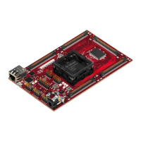
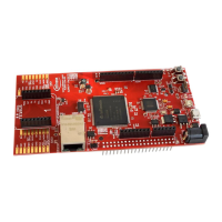
Visual representation of the AURIX™™ lite Kit V2 components and their interconnections.
Details on powering the AURIX™™ lite Kit V2 via DC plug or micro USB.
Description of user push buttons, LEDs, and the potentiometer on the board.
Overview of debugging capabilities using the on-board miniWiggler and connection methods.
Explanation of the reset input pin and methods to issue a reset signal.
Details on the Infineon high-speed CAN transceiver and its connections.
Information on the 2 Kb I2C Serial EEPROM with pre-programmed EUI-48 MAC ID.
Description of the RJ45 connector and the Ethernet PHY for network connections.
Information on assembling optional Cypress Semper™™ NOR Flash devices.
Details on assembling optional Cypress F-RAM serial memory modules.
User startup modes and their selection via Boot Mode Index and hardware configuration.
Details on configurable signals (HWCFG) and their associated resistors.
Mapping of optional resistors to specific signals for enabling/disabling functions.
Available GPIOs and signals at the X1 and X2 pin headers for extension or measurement.
Signal mapping for Shield2Go connectors 1 & 2 and the mikroBus™™ connector.
Mapping of AURIX™™ pin functions to Arduino compatible functions.
Pin assignment of the 10-pin Device Access Port Debug Connector for high-speed debugging.
Schematic overview of the project, including revision history and component placement.
Detailed schematic of the on-board miniWiggler and USB connector circuitry.
Schematic for power supply, analog/digital circuits, and various connectors.
Schematic detailing the CPU, its ports, and hardware configuration signals.
Schematic for the Ethernet interface and optional flash/RAM memory expansion.
Visual representation of component placement on the top side of the board.
Visual representation of component placement on the bottom side of the board.
| Brand | Infineon |
|---|---|
| Model | AURIX lite Kit V2 |
| Category | Motherboard |
| Language | English |