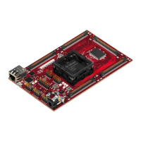
AURIX™ lite Kit V2
Table of Contents
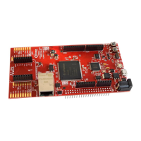
Board Users Manual 4 Revision October, 2020
Table of Contents
1 Introduction ............................................................................................................................. 6
1.1 Block Diagram ...................................................................................................................................... 7
2 Hardware Description ............................................................................................................... 8
2.1 Power Supply ....................................................................................................................................... 9
2.2 User Push Buttons, User LEDs and Potentiometer ............................................................................ 10
2.3 Debugging and on board miniWiggler ............................................................................................... 11
2.3.1 USB Connector ................................................................................................................................... 11
2.3.2 Serial Connection to PC ...................................................................................................................... 11
2.3.3 miniWiggler JDS ................................................................................................................................. 12
2.4 Reset .................................................................................................................................................. 12
2.5 CAN Transceiver ................................................................................................................................. 12
2.6 I2C Eeprom ......................................................................................................................................... 12
2.7 Ethernet ............................................................................................................................................. 13
2.8 Optional Cypress Semper™ (Secure) Flash ........................................................................................ 13
2.9 Optional F-RAM .................................................................................................................................. 13
3 Configuration .......................................................................................................................... 14
3.1 Bootmode .......................................................................................................................................... 14
3.2 Config Signals ..................................................................................................................................... 14
3.3 Optional resistors ............................................................................................................................... 15
4 Connector Pin Assignment ...................................................................................................... 16
4.1 Pinout of X1 and X2 connectors ......................................................................................................... 16
4.2 Shield2Go and MikroBus™ Pinout ..................................................................................................... 17
4.3 Arduino Compatible Connector ......................................................................................................... 18
4.4 Infineon DAP Debug Connector (10-pin) ........................................................................................... 19
5 Schematics and Placement ...................................................................................................... 20
 Loading...