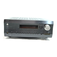
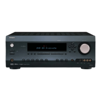
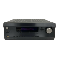
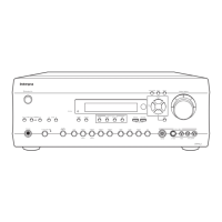
DTR-6.4
MAIN MICROPROCESSOR
TERMINAL DESCRIPTION
No. Symbol I/O Description
51 DSP1BST O Boot strap output pin for first DSP IC.
52 ~DSP1HCS O Serial communication clock output pin for Q302 and Q310.
53 ~DSP1HACN I Acknowledge input pin for first DSP IC.
54 DSP1GP8 O PCM information output pin for first DSP IC.
55 BVdd Power supply pin (3.3V)
56 BVss Ground pin
57 DSP1GP9 I Information input pin to read bit stream information of first DSP IC.
58 GSP1GP10 I Interrupter request input pin for first DSP IC
59 ~DSP2RST O Reset signal output pin for second DSP IC Q703.
60 DSP2BST O Boot strap output pin for second DSP IC.
61 ~CODECRST/~DSPPM O Reset output pin for DIR IC and initializing of PLL of DSP IC
62 ~DSP2HACN I Acknowledge input pin for second DSP IC.
63 DSP2HDOUT I Serial communication data input pin for second DSP IC
64 ~DSP2HCS O Serial communication clock output pin for second DSP IC
65 ~ADPD O Power down output pin for AD converter Q113,4.
66 ADCDIV O Dividing control output pin for AD converter
67 VppEN O Self-write power supply control pin
68 SPZ2 O Speaker relay control output pin for zone 2
69 SPCS O Speaker relay control output pin for center and surround channels
70 SPF O Speaker relay control output pin for front channels
71 Avdd Power supply pin (5V)
72 Avss Ground pin
73 Avref Reference voltage pin for A/D converter
74 VOLH I Output voltage detection input pin of power amplifier
75 ~SD I Broadcast detection input pin
76 ~STEREO I Stereo broadcast detection input pin
77 INIT1 I Initializing pin
78 INIT2 I Initializing pin
79 INIT3 I Initializing pin
80 INIT4 I Initializing pin
81 PROTECT I Abnormal current and voltage detection input pin
82 THRM I Thermal detection input pin
83 SDET I S video detection input pin
84 RDSDA I Data input pin from RDS decoder
85 RDSID I Signal input pin from RDS decoder
86 SYNC I External synchronizing judgment input pin from OSD IC
87 ~VSYNC I Vertical synchronizing signal input pin
88 ~POFF I Power failure detection input pin
89 ~RDSCLK I Clock input pin from RDS decoder
90 ~IRIN I IR signal input pin
91 ~IRZ2 I IR signal input pin for zone 2
92 SEC1H O Power supply control output pin for power amplifier
93 SUBRDY I Ready input pin for sub-microprocessor
94 SUBSDI I Serial communication data input pin for sub-microprocessor
95 SUBSDO O Serial communication data output pin for sub-microprocessor
96 SUBCLK O Serial communication clock output pin for sub-microprocessor
97 232RXD I Not used.
98 232TXD O Not used.
99 ~SUBRST O Reset output pin for sub-microprocessor
100 YCSEPDA O Not used.