HDMI RX Core Signals
ctrl
Output N*6 Note: N = symbols per clock
locked
Output 3
vid_lock
Output 1
in_5v_power
Input 1 HDMI RX 5V detect and hotplug detect
hdmi_rx_hpd_n
Inout 1
I
2
C Signals
hdmi_rx_i2c_sda
Inout 1 HDMI RX DDC and SCDC interface
hdmi_rx_i2c_scl
Inout 1
RX EDID RAM Signals
edid_ram_access
Input 1 HDMI RX EDID RAM access interface.
Assert edid_ram_access when you want
to write or read from the EDID RAM, else
this signal should be kept low.
edid_ram_address
Input 8
edid_ram_write
Input 1
edid_ram_read
Input 1
edid_ram_readdata
Output 8
edid_ram_writedata
Input 8
edid_ram_waitrequest
Output 1
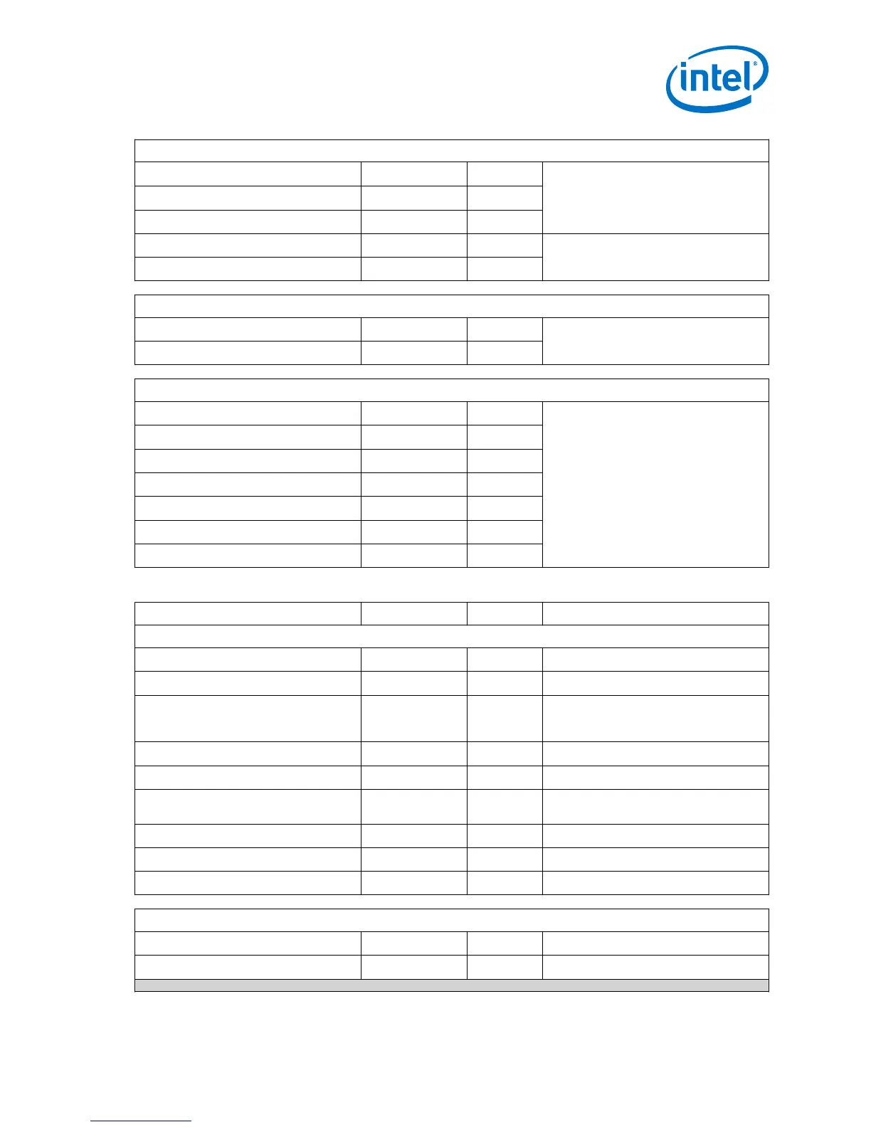
Table 17. HDMI TX Top-Level Signals
Signal Direction Width Description
Clock and Reset Signals
mgmt_clk
Input 1 System clock input (100 MHz)
reset
Input 1 System reset input
hdmi_clk_in
Input 1 Reference clock to TX IOPLL and TX PLL.
The clock frequency is the same as the
TMDS clock frequency.
vid_clk_out
Output 1 Video clock output
ls_clk_out
Output 8 Link speed clock output
sys_init
Output 1 System initialization to reset the system
upon power-up
reset_xcvr
Input 1 Reset to TX transceiver
reset_pll
Input 1 Reset to IOPLL and TX PLL
reset_pll_reconfig
Output 1 Reset to PLL reconfiguration
TX Transceiver and IOPLL Signals
tx_serial_data
Output 4 HDMI serial data from the TX Native PHY
gxb_tx_ready
Output 1 Indicates TX Native PHY is ready
continued...
2 Intel FPGA HDMI Design Example Detailed Description
UG-20077 | 2017.11.06
Intel
®
FPGA HDMI Design Example User Guide for Intel
®
Arria 10 Devices
29
 Loading...