RX-DP10VBK/RX-DP10VSL
RX-DP10RSL
1-18
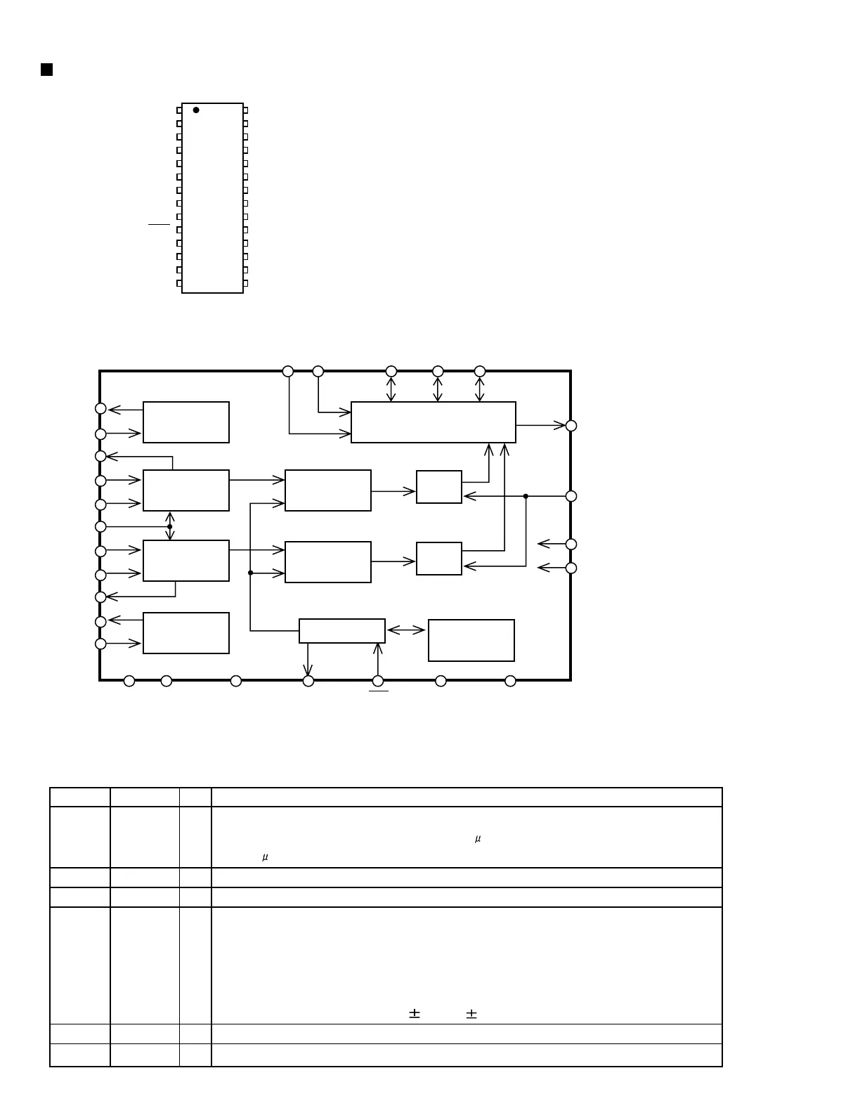
1. Pin layout
2. Block diagram
AK5383VF (IC657) : A/D converter
VREFL
GNDL
VCOML
AINL+
AINL-
ZCAL
AINR+
AINR-
VCOMR
VREFR
GNDR
SDATA
HPFE
MCLK
DFS
1
2
3
4
5
6
25
24
26
28
27
Voltge
Reference
Voltge
Reference
Delta-Sigma
Mdulator
Delta-Sigma
Mdulator
Serial Output
Interface
Decimation
Filter
Decimation
Filter
Controller
HPF
HPF
Calibration
SRAM
SMODE1 SMODE2 SLCK LRCK FSYNC
12 11 14 13 16
15
19
17
18
23 22 21 9 10 7 8
VA AGND BGND CAL RST VD DGND
VRFEL
GNDL
VCOML
AINL+
AINL-
ZCAL
VD
DGND
CAL
RST
SMODW2
SMODE1
LRCK
SCLK
VREFR
GNDR
VCOMR
AINR+
AINR-
VA
AGND
BGND
TEST
HPFE
DFS
MCLK
FSYNC
SDATA
1
2
3
4
5
6
7
8
9
10
11
12
13
14
28
27
26
25
24
23
22
21
20
19
18
17
16
15
3. Pin function (1/2)
Pin name
VRFEL
GNDL
VCOML
AINL+
AINL-
ZCAL
VD
DGND
I/O
O
-
O
I
I
I
-
-
Function
Lch Reference Voltage Pin, 3.75V
Normally connected to GNDL with a 10 F electrolytic capacitor and
a 0.1 F ceramic capacitor.
Lch Reference Ground Pin, 0V
Lch Common Voltage Pin, 2.75V
Lch Analog positive input Pin
Lch Analog negative input Pin
Zero Calibration Control Pin
This pin controls the calibration reference signal.
"L": VCOML and VCOMR
"H": Analog Input Pins (AINL , AINR )
Digital Power Supply Pin, 3.3V
Digital Ground Pin, 0V
Pin No.
1
2
3
4
5
6
7
8