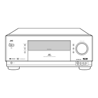
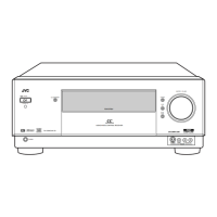
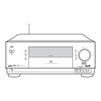
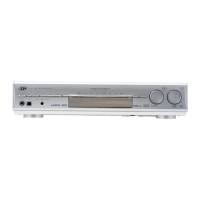
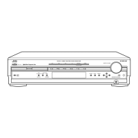
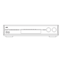
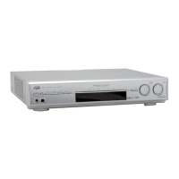
RX-DP10VBK/RX-DP10VSL
RX-DP10RSL
1-19
Pin name
CAL
RST
SMODE2
SMODE1
LRCK
SCLK
SDATA
FSYNC
MCLK
DFS
HPFE
TEST
BGND
AGND
VA
AINR-
AINR+
VCOMR
GNDR
VREFR
I/O
O
I
I
I
I/O
I/O
O
I/O
I
I
I
I
-
-
-
I
I
O
-
O
Function
Calibration Active Signal Pin
"H" means the offset calibration cycle is in progress. Offset calibration starts
when RST goes "H". CAL goes "L" after 8704 LRCK cycles for DFS="L",
17408 LRCK cycles for DFS="H".
Reset Pin
When "L", Digital section is powered-down. Upon returning "H", an
offset calibration cycle is started. An offset calibration cycle should always
be initiated after power-up.
Serial Interface Mode Select Pin
MSB first, 2's compliment.
Left/Right Channel Select Clock Pin
LRCK goes "H" at SMODE2="L" and "L" at SMODE2="H" during reset
when SMODE1 "H".
Serial Data Clock Pin
Data is clocked out on the falling edge of SCLK.
Slave mode:
SCLK requires more than 48fs clock.
Master mode:
SCLK outputs a 128fs(DFS="L") or 64fs (DFS="H")clock.
SCLK stays "L" during reset.
Serial Data Output Pin
MSB first, 2's complement. SDATA stays "L" during reset.
Frame Synchronization Signal Pin
Slave mode:
When "H", the data bits are clocked out on SDATA. In I2S mode, FSYNC is
Don't care.
Master mode:
FSYNC outputs 2fs clock. FSYNC stays "L" during reset.
Master Clock Input Pin
256fs at DFS="L", 128fs at DFS="H".
Double Speed Sampling mode Pin
"L": Normal Speed "H": Double Speed
High Pass Filter Enable Pin
"L": Disable "H": Enable
Test Pin (pull-down pin)
Should be connected to GND.
Substrate Ground Pin, 0V
Analog Ground Pin, 0V
Analog Supply Pin, 5V
Rch Analog negative input Pin
Rch Analog positive input Pin
Rch Common Voltage Pin, 2.75V
Rch Reference Ground Pin, 0V
Rch Reference Voltage Pin, 3.75V
Normally connected to GNDR with a 10 F electrolytic capacitor and a 0.1 F
ceramic capacitor
SMODE2
L
L
H
H
SMODE1
L
H
L
H
MODE
Slave mode : MSB justified
Master mode : Similar to I2S
Slave mode :I2S
Master mode : I2S
LRCK
: H/L
: H/L
: L/H
: L/H
Pin No.
9
10
11
12
13
14
15
16
17
18
19
20
21
22
23
24
25
26
27
28
3. Pin function (2/2)
Note: All digital inputs should not be left floating.