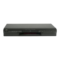
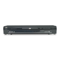
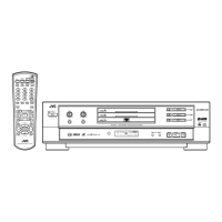
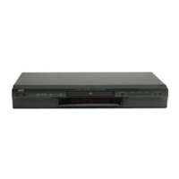
XV-S300BK/XV-S332SL/XV-S402SL/XV-S403SG
32
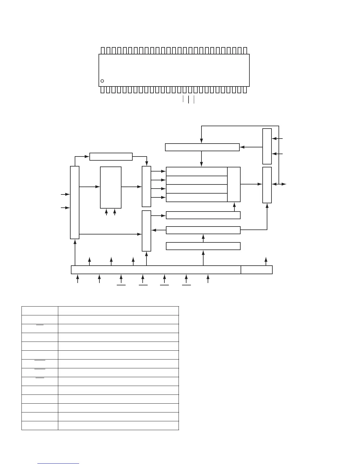
4.9 K4S641632F-TC75 (IC504) :CMOS SDRAM
4.9.1 Pin layout
4.9.2 Block diagram
4.9.3 Pin functions
Vcc
DQ0
Vcc
Q
DQ1
DQ2
V
SSQ
DQ3
DQ4
Vcc
Q
DQ5
DQ6
V
SSQ
DQ7
Vcc
LDQM
WE
CAS
RAS
CS
BS0
BS1
10/AP
A0
A1
A2
A3
Vcc
V
SS
DQ1
V
SSQ
DQ1
DQ1
Vcc
Q
DQ1
DQ1
V
SSQ
DQ1
DQ9
Vcc
Q
DQ8
V
SS
N.C
UDQ
CLK
CKE
NC
A11
A9
A8
A7
A6
A5
A4
V
SS
1
2
3
4
5
6
7
8
9
10
11
12
13
14
15
16
17
18
19
20
21
22
23
24
25
26
27
54
53
52
51
50
49
48
47
46
45
44
43
42
41
40
39
38
37
36
35
34
33
32
31
30
29
28
Bank select
Address register
Row buffer
Refresh counter
Row decoder
Col. buffer
LK
DD
LCBR
LRAS
LCKE
LRAS LCBR LWE LCAS
CLK CKE CS RAS CAS WE L(U)DQM
Timing register
LWCBR
LDQM
Programming register
Latency & Burst length
Column decoder
1M x 16
1M x 16
1M x 16
1M x 16
Data input register
Sense AMP.
I/O Control Output buffer
LWE
LDQ
DQ
Symbol Description
CLK System clock
CS
Chip select
CKE Clock enable
A0~A11 address
BS0,1 Bank address strobe
RAS
Row address strobe
CAS
column address strobe
WE
Write enable
LDQM Data input/output mask
DQ0~15 Data input/output
Vcc/Vss Power supply/ground
Vccq/Vssq Data output power/ground
N.C Non connect
 Loading...