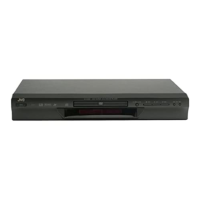
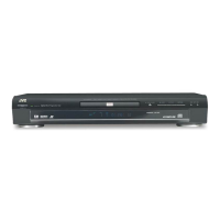
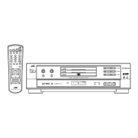
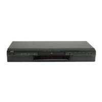
XV-S300BK/XV-S332SL/XV-S402SL/XV-S403SG
40
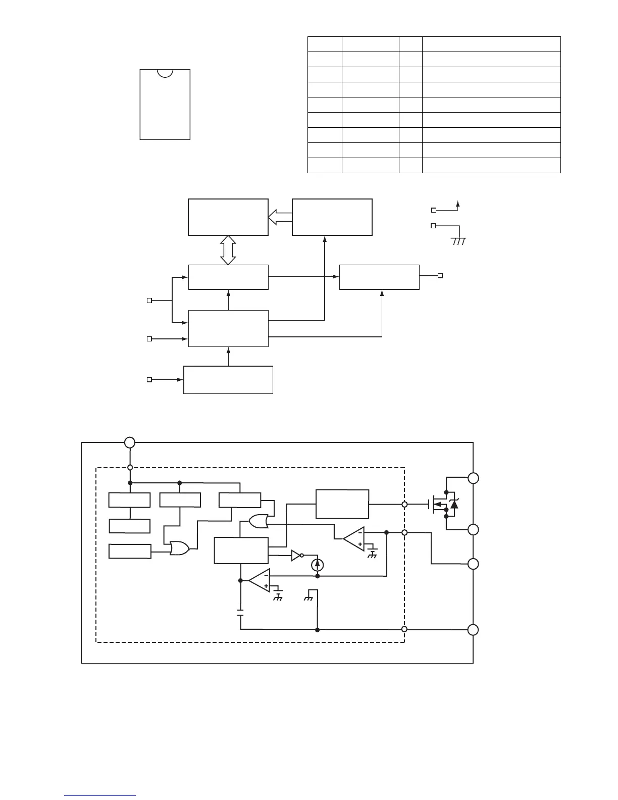
4.15S-93C66AFJ-X (IC451) : EEPROM
4.15.1 Pin layout
4.15.2 Pin function
4.15.3 Block diagram
4.16STR-G6551-F8 (IC901) : Switch regulator
1
2
3
4
8
7
6
5
PE
CC
CS
SK
NC
GN
DO
DI
Pin No. Symbol I/O Description
1 PE - Non connect
2 VCC - Power supply terminal
3 CS I Chip select input
4 SK I Serial clock input
5 DI I Serial data input
6 DO O Serial data output
7 GND - Connect to ground
8 NC - Non connect
DI
S
K
DO
Vcc
GND
Memory
array
Address
decoder
Data resister
Mode decode
logitech
Clock generation
circuit
Buffer output
D
2
1
S
5
3
O.C.P/F
GND
Comp.2
4
START
REG
T.S.D
O.V.P
LATCH
O.S.C
Vth(2)
DRIVE
Comp.1
Vth(1)
 Loading...