XV-S300BK/XV-S332SL/XV-S402SL/XV-S403SG
41
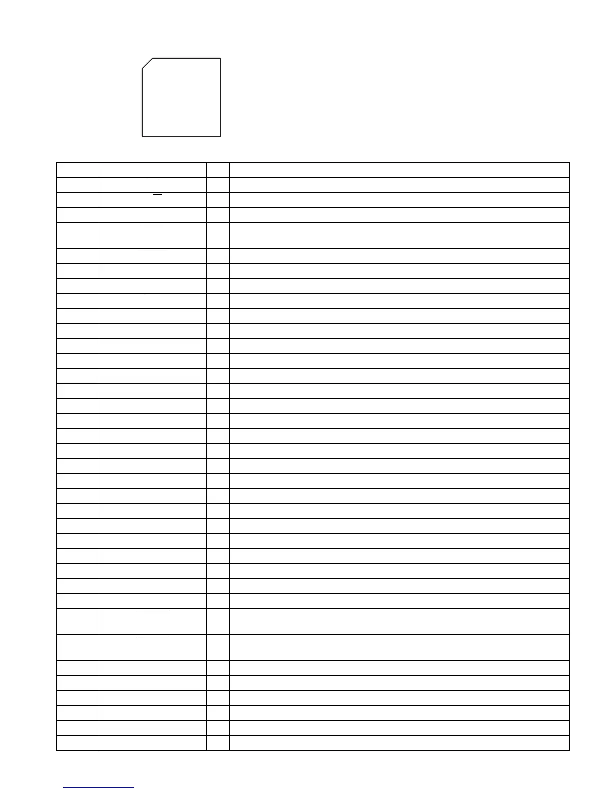
4.17ZIVA-4.1-PB0 (IC501) : Back end - Digital decoder
4.17.1 Terminal layout
4.17.2 Pin function (1/5)
1
52
15
10
208 157
53 104
~
~
~
~
Pin No. Symbol I/O Description
1RD
I Read strobe input
2 R/W I Read/write strobe input
3 VDD_3.3 - Power supply terminal 3.3V
4WAIT
O Transfer not complete / data acknowledge.
Active LOW to indicate host initiated transfer is complete.
5 RESET
I Active LOW : reset signal input
6 VSS - Connect to ground
7 VDD_3.3 - Power supply terminal 3.3V
8INT
O Host interrupt signal output
9 NC - Non connect
10 NC - Non connect
11 NC - Non connect
12 NC - Non connect
13 VDD_2.5 - Power supply terminal 2.5V
14 VSS - Connect to ground
15 NC - Non connect
16 NC - Non connect
17 NC - Non connect
18 NC - Non connect
19 VSS - Connect to ground
20 VDD_3.3 - Power supply 3.3V
21 VDATA0 O Video data bus output. Byte serial CbYCrY data synchronous with VCLK.
22 VDATA1 O Video data bus output. Byte serial CbYCrY data synchronous with VCLK.
23 VDATA2 O Video data bus output. Byte serial CbYCrY data synchronous with VCLK.
24 VDATA3 O Video data bus output. Byte serial CbYCrY data synchronous with VCLK.
25 VDATA4 O Video data bus output. Byte serial CbYCrY data synchronous with VCLK.
26 VDATA5 O Video data bus output. Byte serial CbYCrY data synchronous with VCLK.
27 VDATA6 O Video data bus output. Byte serial CbYCrY data synchronous with VCLK.
28 VDATA7 O Video data bus output. Byte serial CbYCrY data synchronous with VCLK.
29 VSYNC
I/O Vertical sync. Bi-directional, the decoder output the top border of a new
field on the first HSYNC after the falling edge of VSYNC.
30 HSYNC
I/O Horizontal sync. The decoder begins outputting pixel data for a new
horizontal line after the falling (active) edge of HSYNC.
31 VSS - Connect to ground
32 VDD_3.3 - Power supply terminal 3.3V
33 NC - Non connect
34 NC - Non connect
35 NC - Non connect
36 VDD_2.5 - Power supply terminal 2.5V

 Loading...