NXR-800
17
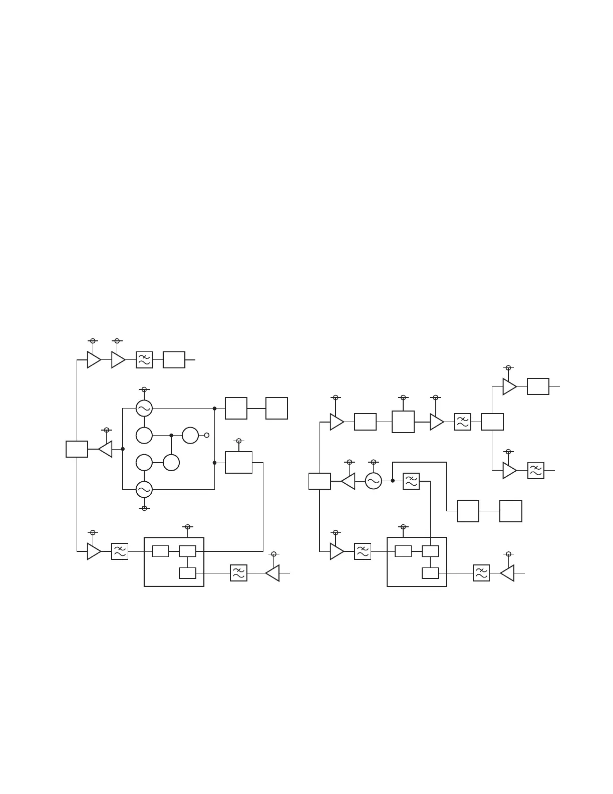
4-7. Receiver PLL circuits
The receiver unit (X55-310) has the 1st-PLL circuit for
controlling the VCO that generates the hetero signal to the
first local oscillator, and the 2nd-PLL circuit for controlling
the VCO that generates the hetero signal to the second local
oscillator.
The 1st-PLL circuit consists of the VCO (Q7 and Q8),
the Buffer amplifi er (Q17), the RF amplifi ers (Q16 and Q3),
the PLL-IC (IC5), the Active loop fi lters (Q2 and Q4) and the
Band switches (Q14, Q10, Q11 and Q59). The signal in the
318.05~334.00MHz band generated by VCO Q7 and the
334.05~350.05MHz band generated by VCO Q8 is input to
IC5 (pin5) via Q17 and Q16 as the Fin signal. The 6MHz
reference signal generated by the DDS-IC (IC7) is input to
IC5 (pin8) via Q3. Two signals, Fin and REFin, are phase-
compared as the 100kHz comparison frequency by each
frequency divider. The VCO output with the frequency syn-
chronized is input to the 1st-Mixer as the fi rst local oscillator
Lower hetero signal approximately +17dBm via Q17, Q23,
and Q18. The control voltage is input to IC30 (ADC) pin16
via IC6.
Meanwhile, the 2nd-PLL circuit consists of the VCO (Q24),
the Buffer amplifier (Q33), the RF amplifier (Q38, Q22),
and the PLL-IC (IC11). The 99.0MHz signal generated by
Q24 is input to IC11 (pin5) as the Fin signal via Q38. The
19.2MHz Internal reference clock distributed by the transmit-
ter unit (X56-312) is input as the REFin signal to IC11 (pin8)
via Q22. Two signals, Fin and REFin, are phase-compared
by each frequency divider as the comparison frequency of
200kHz. The VCO output with the frequency synchronized
is input to IC9 (prescaler IC) pin2 via Q33 and Q21. The
49.5MHz signal is frequency-divided into halves by IC9 and
is excited by Q53 and distributed. One is input to IC12 (pin1)
via Buffer amplifi er_Q35. The other is input to IC13 (pin4)
via Buffer amplifi er_Q36. Both are input as approximately
–16dBm for the second local oscillator Lower hetero signal.
The control voltage at this point is input to IC30 (ADC) pin10
via IC33.
4-8. AVR circuit
The power supply voltage supplied from the power unit
(X45-382 C/5) is distributed from the receiver unit (X55-310)
CN44 to IC24 (8V), IC25 (8V), IC26 (9V), and IC27 (9V) via
the Q52 DC switch. The output of IC24 is supplied to the
1st-IF circuits, the 1st-Local amplifi ers and the IF system IC_
IC12 via IC15 (5V). Further, the output of IC25 is distributed
to IC16 (5V), IC17 (5V), IC18 (5V) and IC19 (5V). The out-
put of IC16 is supplied to IF system IC_IC13. The output of
IC17 is supplied to the 2nd-Local amplifi ers. The output of
IC18 is supplied to the 1st-PLL and the 2nd-PLL. The output
of IC19 is supplied to the DDS circuit. The output of IC26 is
supplied to LNA_Q1. The output of IC27 is supplied to the
VCO buffer amplifi ers_Q17, Q33, the 1st-VCO and the 2nd-
VCO via Active ripple fi lters_Q9, Q27, and to the Active loop
fi lter_Q2, Q4 via the Active ripple fi lters_Q6.
Fig. 21 Receiver PLL circuits
CIRCUIT DESCRIPTION
Q17
1/N
1/R
PD
+5V
+5V
+9V
Q3
+5V
20
8
IC5
5
Fin
LPF
LPF
Q16
+8V
LPF
Q23
+8V
Q18
REFin
+9LV
+9LV
+9LV
+9LV
SW
SW
Q10
SW SW
Q11
Q14
Q59
Q7
318.05~334.00MHz
Q8
334.05~350.05MHz
Div.
Active
LPF
IC6
16
IC30
ADC
IC9
1/2
IC33
10
IC30
ADC
Q2,4
Q33
1/N
1/R
PD
+5V
+5V
+9V
Q22
+5V
20
8
IC11
5
Fin
LPF
LPF
LPF
LPF
LPF
Q38
+5V
Q21
+5V+3V
Q53
+5VA
Q35
+5VD
Q36
REFin
Div.
Div.
ATT
ATT
ATT
Q24
99.0MHz
27
49.5MHz

 Loading...