NXR-800
16
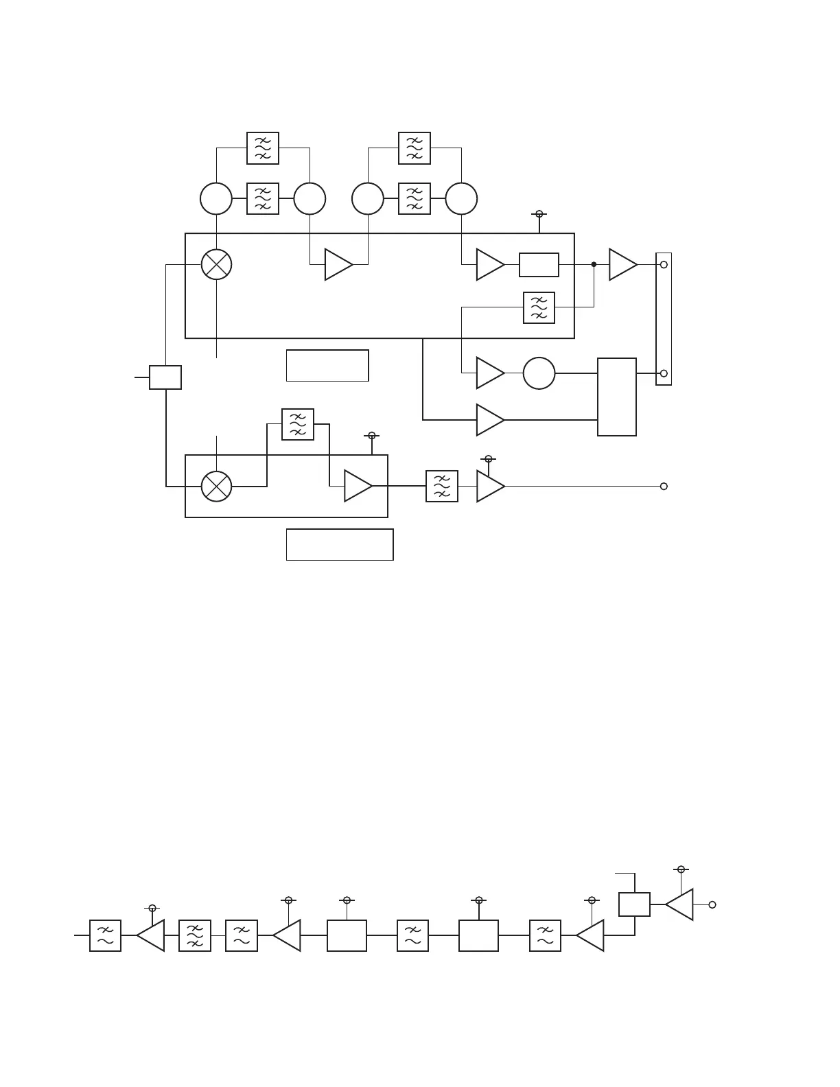
4-5. Squelch circuit
The desired noise of the noise component output from IF
system IC_IC12 (pin 18) is extracted by the BPF. After pass-
ing through Q40, it is DC-detected as the squelch voltage by
D17, D18 and input to ADC_IC30 (pin 11).
The MPU mounted in the control unit (X53-413) com-
pares it with a predetermined reference voltage and turns
the Audio signal on and off. The strength of the receiver
signal input from CN5 is output as the RSSI voltage from IF
system IC_IC12 (pin 21), and is input to_IC30 (ADC) pin 12
via IC29 A/2.
4-6. Receiver DDS circuit
The 19.2MHz Internal reference clock produced by trans-
mitter unit (X56-312 A/3) is distributed to CN45 of the re-
ceiver unit (X55-310). It passes through Q39, Q30, and IC8,
and is input to IC7 (DDS-IC) pin 6 as the Master clock. Ap-
proximately 6MHz signal is generated as the 1st-PLL Refer-
ence clock.
IC7 has a resolution of 32 bits for realizing the frequency
step minters than the 1st-PLL comparison frequency. The
generated Reference clock is output via Q12, CF1, and Q5.
CF1 is a Ceramic Filter. It is the BPF for removing unneces-
sary spurious noise included in the generated Reference
clock.
D15
SW
D16
SW
CF2
CF3
D19
SW
D20
SW
DET
CF5
CF7
QUAD
10
864
15
17
IC20
(A/2)
Q40
IC29 (A/2)
D17,18
IC30
11 18
12
1821
24
1
48 10
DIV
2nd local
49.5MHz
2nd local
49.5MHz
6
CF4
CF6
14
5DR
3DR
5NR
Analog Wide
Analog Narrow
NXDN Narrow
NXDN Very-Narrow
IC12
IC13
IC14
CN42
12
22
CN43
LPF LPF LPF LPFBPF
+5V
Q5
+5V +5V
Q12
+5V
Q30
+5V
Q39
CF1
IC7
DDS
14
6
+5V
IC8
1
5
DIV
CN45
Fig. 19 Demodulator circuits
Fig. 20 Receiver DDS circuit
CIRCUIT DESCRIPTION

 Loading...