CrossLink Programming and Configuration Usage Guide
Technical Note
© 2015-2017 Lattice Semiconductor Corp. All Lattice trademarks, registered trademarks, patents, and disclaimers are as listed at www.latticesemi.com/legal. All other brand or product names are
trademarks or registered trademarks of their respective holders. The specifications and information herein are subject to change without notice.
FPGA-TN-02014-1.2 11
Table 4.3. Default State of sysCONFIG Pins
Feature Row Blank Mode
(Configuration Mode)
in User Mode
(Software Default
State)
Note: All pins are in Configuration Mode until the device is configured and enters User Mode.
Table 4.4. Default State in Diamond for each Port
1. This default setting can be modified in the Diamond Spreadsheet View, Global Preferences tab.
2. The MASTER_SPI_PORT setting does not influence the behavior during configuration. For details, see the Configuration
section.
4.10.1. Self-Download Port Pins
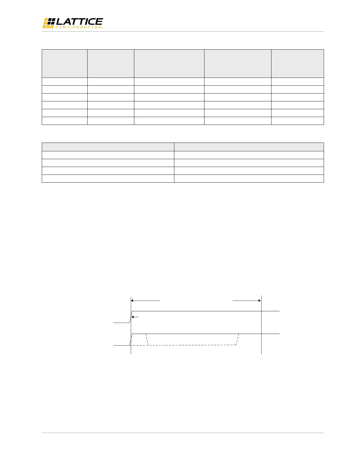
CRESETB
The CRESETB is an active LOW input with a weak internal pull-up resistor used for configuration the FPGA. When
CRESETB is asserted LOW, the FPGA exits User Mode and starts a device configuration sequence at the Initialization
phase, as described in Figure 4.1. Holding the CRESETB pin LOW during power up keeps CrossLink in the Initialization
phase. This LOW period also allows an external SPI Master or I
2
C Master to write the Activation Key to the FPGA to
enter into slave configuration mode. The CRESETB has a minimum pulse width assertion period in order for it to be
recognized by the FPGA. You can find this minimum time in CrossLink Family Data Sheet (FPGA-DS-02007) in the AC
timing section.
CRESETB
VCC VCC min.
CRESETB transitions observed
Figure 4.2. Period CRESETB is Always Observed