CrossLink Programming and Configuration Usage Guide
Technical Note
© 2015-2017 Lattice Semiconductor Corp. All Lattice trademarks, registered trademarks, patents, and disclaimers are as listed at www.latticesemi.com/legal. All other brand or product names are
trademarks or registered trademarks of their respective holders. The specifications and information herein are subject to change without notice.
FPGA-TN-02014-1.2 7
4. Configuration Process and Flow
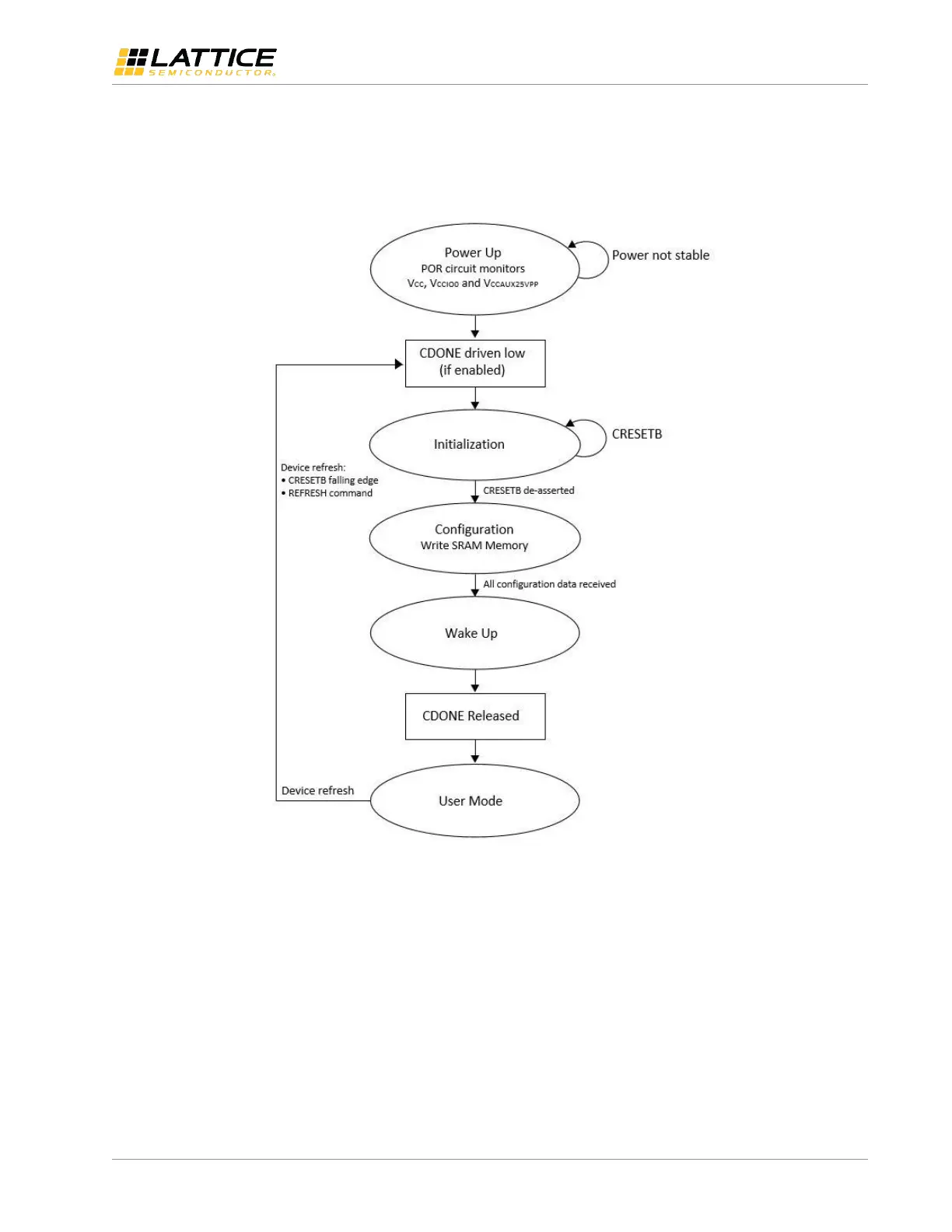
Before it is operational, the FPGA goes through a sequence of states, including initialization, configuration and wake-
up. Figure 4.1 shows the configuration flow.
Figure 4.1. Configuration Flow
The CrossLink sysCONFIG ports provide industry standard communication protocols for programming and configuring
the FPGA. Each protocol provides a way to access the CrossLink device’s internal NVCM, or to load its configuration
SRAM.
The sysCONFIG ports capable of accessing the NVCM have a priority order. The MSPI configuration port does not have
the ability to alter the NVCM space, and as a result is not a factor in the sysCONFIG port priority scheme.