CrossLink Programming and Configuration Usage Guide
Technical Note
© 2015-2017 Lattice Semiconductor Corp. All Lattice trademarks, registered trademarks, patents, and disclaimers are as listed at www.latticesemi.com/legal. All other brand or product names are
trademarks or registered trademarks of their respective holders. The specifications and information herein are subject to change without notice.
22 FPGA-TN-02014-1.2
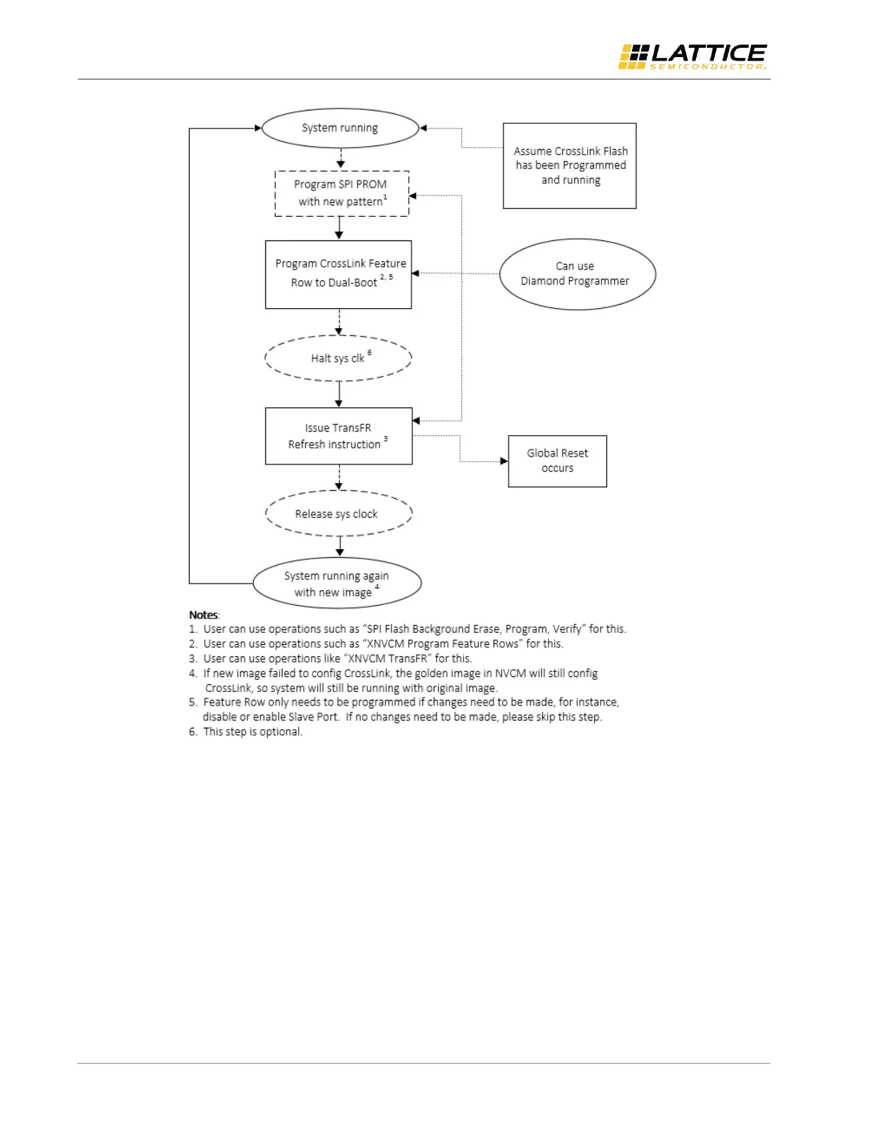
Figure 5.4. Example Process Flow
Caution when using the above process flow:
As a Global Reset is triggered during device wake-up after Refresh instruction is issued, attention needs to be given in
designing I/O with following conditions:
Register output pins
Impact on the system board level when value changes (may shut off the board, for instance)
Register is set/reset by global reset
For the I/O in the example above, the state of the I/O is not changed during the TransFR refresh, but may change when
the device gets into User Mode right after the TransFR refresh. Following are design tips to avoid this:
For critical I/Os, do not use global reset
For critical I/Os, if you have to use global reset, use the set/reset option so that when GSR occurs, the state of the
I/O pin does not trigger a system crash.