CrossLink Programming and Configuration Usage Guide
Technical Note
© 2015-2017 Lattice Semiconductor Corp. All Lattice trademarks, registered trademarks, patents, and disclaimers are as listed at www.latticesemi.com/legal. All other brand or product names are
trademarks or registered trademarks of their respective holders. The specifications and information herein are subject to change without notice.
20 FPGA-TN-02014-1.2
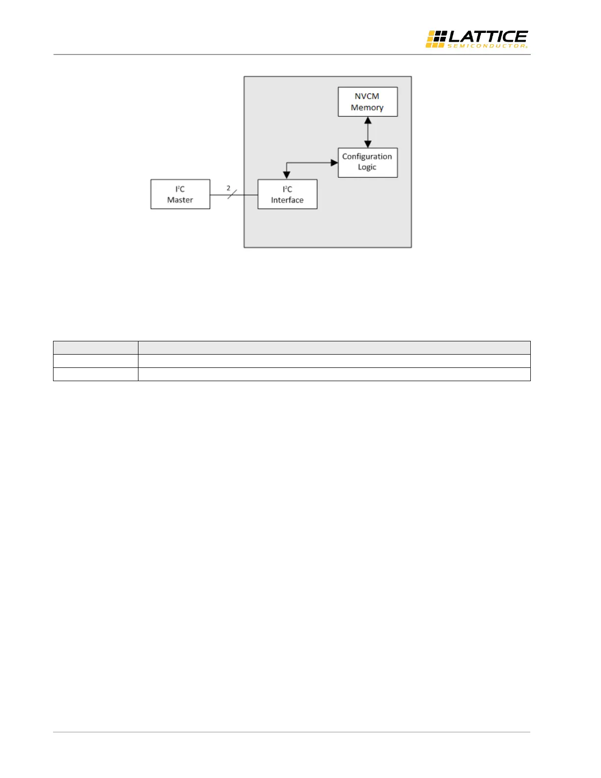
Figure 5.2. I
2
C Configuration Logic
An external I
2
C Master accesses the Configuration Logic using address 1000000 (7-bit mode) or 1111000000 (10- bit
mode) unless the I
2
C base address has been modified.
Table 5.6 lists the address decoding used to access the I
2
C resources in CrossLink.
Table 5.6. Slave Addresses for I
2
C Ports
Primary I
2
C Controller Configuration Logic address. Always responds to 7-bit or 10-bit addresses.
Primary I
2
C Configuration Logic Reset. Always responds to 7-bit or 10-bit addresses.
Note: Although there are four possible combinations of the reserved address bits 1000 0XX, only the two combinations listed
above are used. The remaining two addresses are reserved for future I
2
C bus enhancements.
The CrossLink I
2
C controller supports two separate slave addresses as listed in Table 5.6. These are determined by the
two least significant bits in the slave address – 00 corresponds to the Configuration Logic, while 11 corresponds to a
reset port. In some instances, an I
2
C memory transaction to the Configuration Logic may be interrupted or abandoned.
It is possible for a command to be accepted by the Configuration Logic that causes the Configuration Logic to respond
with data. In the event that the I
2
C memory transaction is interrupted or abandoned, the Configuration Logic continues
to return the queued data.
New incoming I
2
C commands may be considered padding bytes or may be misinterpreted. Clear this condition by
writing any value to the address with least significant bits 11. The Configuration Logic command interpreter is reset,
any queued data is flushed, and subsequent I
2
C memory transactions to the Configuration Logic operates correctly.