MIPI D-PHY Bandwidth Matrix Table
User Guide
© 2015-2018 Lattice Semiconductor Corp. All Lattice trademarks, registered trademarks, patents, and disclaimers are as listed at www.latticesemi.com/legal.
All other brand or product names are trademarks or registered trademarks of their respective holders. The specifications and information herein are subject to change without notice.
16 FPGA-UG-02041-1.1
6. Device Selection
This section summarizes Lattice FPGA families that support MIPI interface with external components as described in
the MIPI CSI-2/DSI Interfaces section.
6.1. Hardware Features
Table 6.1 highlights the features of MIPI D-PHY hardware implementation using MachXO2, MachXO3L, LatticeECP3,
ECP5/ECP5-5G and Crosslink device families. For more details on MIPI D-PHY Receiver and Transmitter resource
utilization and design performance, refer to the MIPI D-PHY Interface IP (RD1182) document.
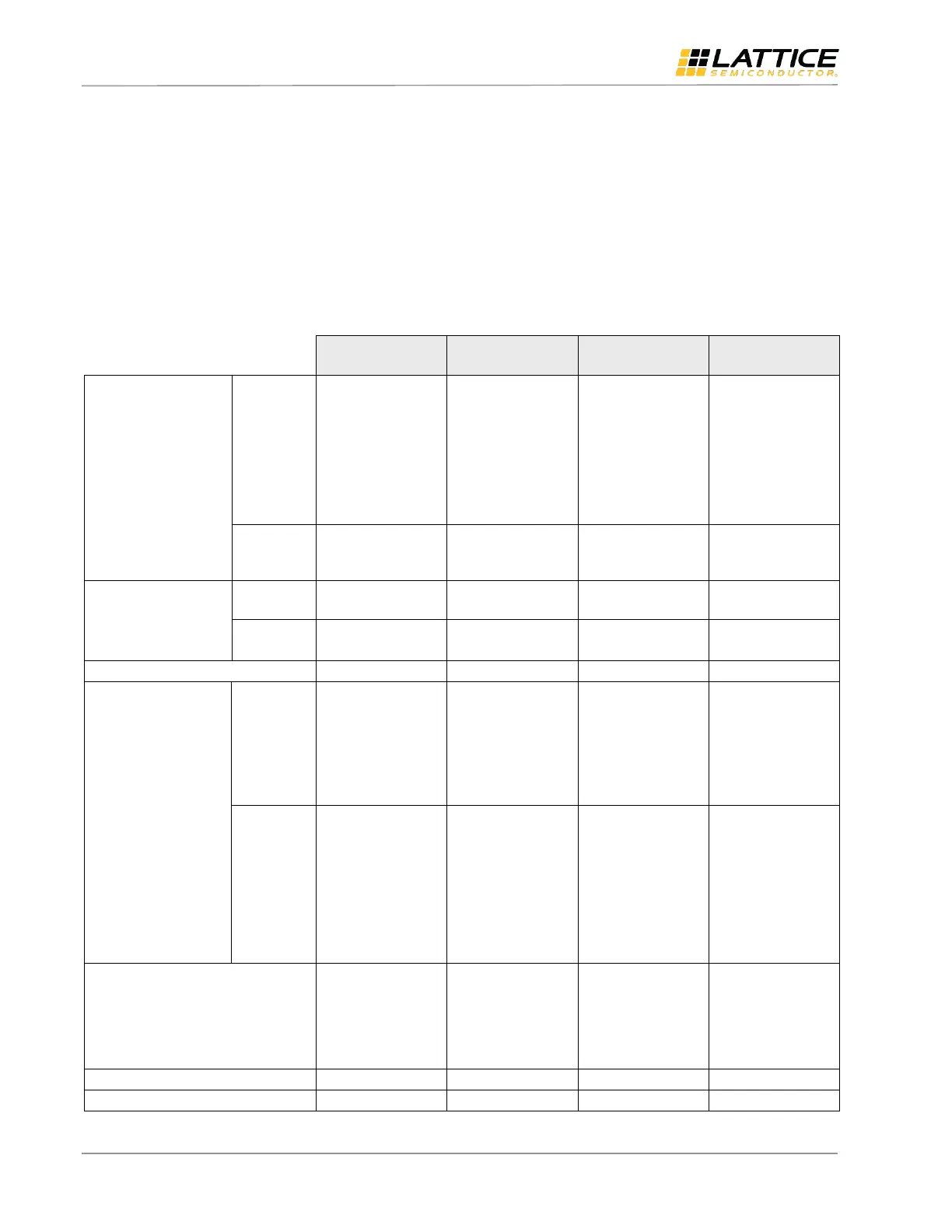
Table 6.1. MIPI Soft D-PHY RX/TX Hardware Comparison
MIPI D-PHY
Rx Implementations
VCCIO = 2.5 V
or 3.3 V
Internal 100 Ω
differential
termination.
VCCIO = 2.5v
or 3.3v
Internal 100 Ω
differential
termination.
VCCIO = 2.5 V
or 3.3 V
Internal 100 Ω
differential
termination.
Dedicated
MIPI D-PHY
inputs buffer
Internal 100 Ω
differential
termination
Dedicated
MIPI D_PHY
input buffer
MIPI D-PHY Tx
Implementations
Up to two RX D-
PHYs; Bank 2 only.
Up to two RX D-
PHYs. Only two
clock divider
primitives, one on
Bank 2 or 3 (right),
one on Bank 6 or 7
(left)
Up to 4 RX D-PHYs
(left and right sides)
Four dedicated
Clock Divider
(CLKDVI) available
Limited by PIO pairs
and clock divider
available in Bank 1
and 2 only
TX D-PHY max
limited by PIO A/B
pairs; Bank 0 only
TX D-PHY maximum
limited by PIO pairs
available in Bank 2,
3, 6 and 7 if CLKDIV
is shared on each
side. If TX D-PHY on
side, can only have
RX D-PHY on the
other
TX D-PHY maximum
limited by PIO
pairs, available in
the left and right
banks.
Depends on data
rate and number of
PIO A/B pairs
available. DDRX4
requires A/B pair
and Edge clock
Depends on data
rate and number of
PIO A/B pairs
available. DDRX4
requires A/B pair
and Edge clock
Depends on data
rate and number of
PIO A/B pairs
available. DDRX4
requires A/B pair
and Edge clock


 To Next Page