MIPI D-PHY Bandwidth Matrix Table
User Guide
© 2015-2018 Lattice Semiconductor Corp. All Lattice trademarks, registered trademarks, patents, and disclaimers are as listed at www.latticesemi.com/legal.
All other brand or product names are trademarks or registered trademarks of their respective holders. The specifications and information herein are subject to change without notice.
22 FPGA-UG-02041-1.1
7.2. FPGA Transmitter Interface
7.2.1. MachXO2/MachXO3L
Maximum MIPI compliance data rate calculation for MachXO2/MachXO3L:
0.206 = 0.15 x UI
UI = 0.206/0.15 = 1.373 ns
Max Data Rate = 1/UI = 1/1.373 = 728 Mbps (at 0.15 UI)
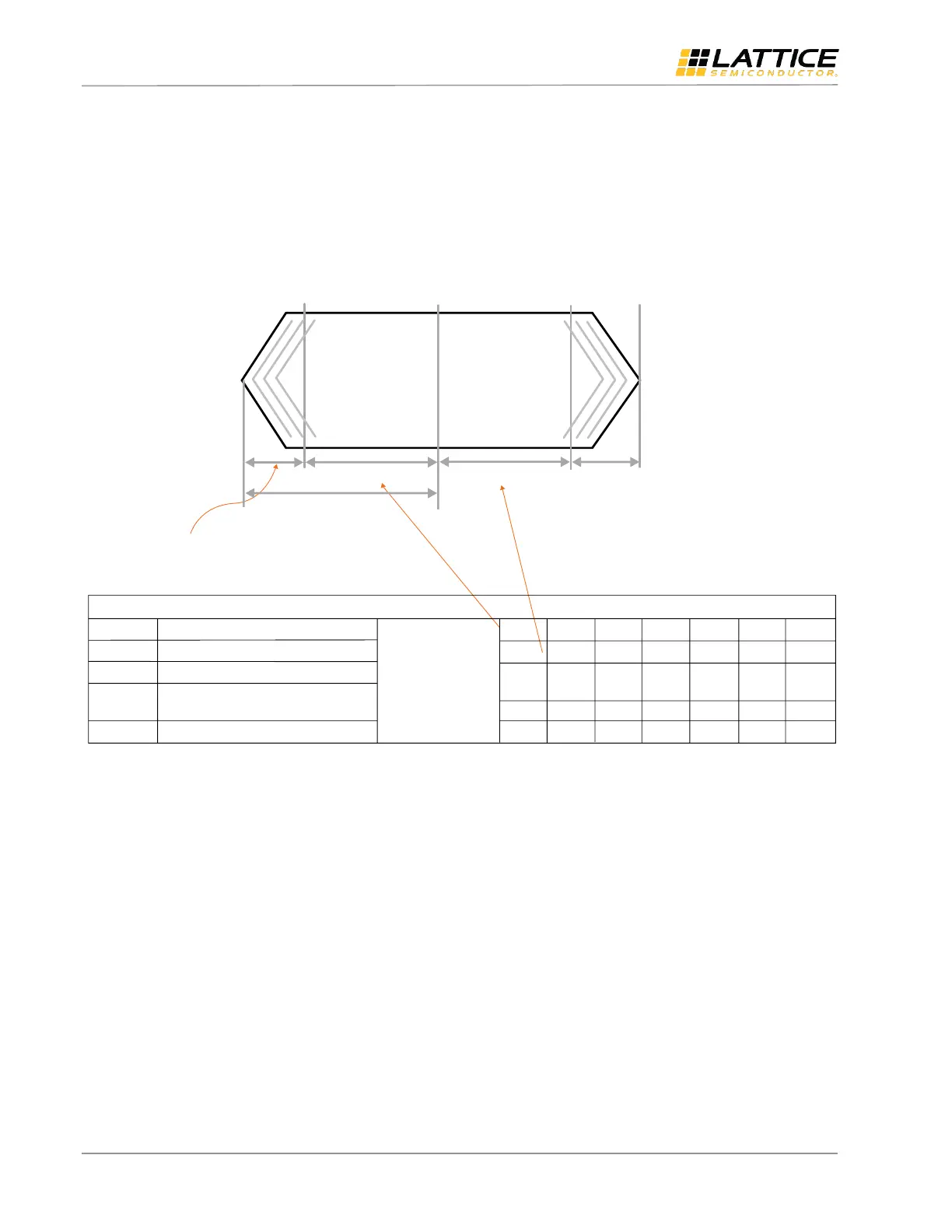
Setup Time
Hold Time
0.455
0.455
At 756 Mbps, ½ UI = 0.661
Tskew = 0.661 - 0.445 = 0.206
MachXO2 Data Sheet Rev. 3.3 at 756 Mbps
Generic DDRX4 Outputs with Clock and Data Centered at Pin Using PCLK Pin for Clock Input – GDDRX4TX.ECLK.Centered
t
DVB
Output Data Valid Before CLK Output
MachXO2-640U,
MachXO2-1200/U
and larger devices,
top side only
t
DVA
Output Data Hold After CLK Output
f
DATA
DDRX4 Serial Output Data Speed
f
DDRX4
DDRX4 ECLK Frequency
(minimum limited by PLL)
f
SCLK
SCLK Frequency
0.455
0.455
756
378
95
—
—
—
—
—
0.570
0.570
630
315
79
—
—
—
—
—
0.710
0.710
524
262
66
—
—
—
—
—
Mbps
MHz
MHz
ns
ns
Figure 7.5. MachXO2 Maximum Data Rate
 Loading...