MIPI D-PHY Bandwidth Matrix Table
User Guide
© 2015-2018 Lattice Semiconductor Corp. All Lattice trademarks, registered trademarks, patents, and disclaimers are as listed at www.latticesemi.com/legal.
All other brand or product names are trademarks or registered trademarks of their respective holders. The specifications and information herein are subject to change without notice.
FPGA-UG-02041-1.1 9
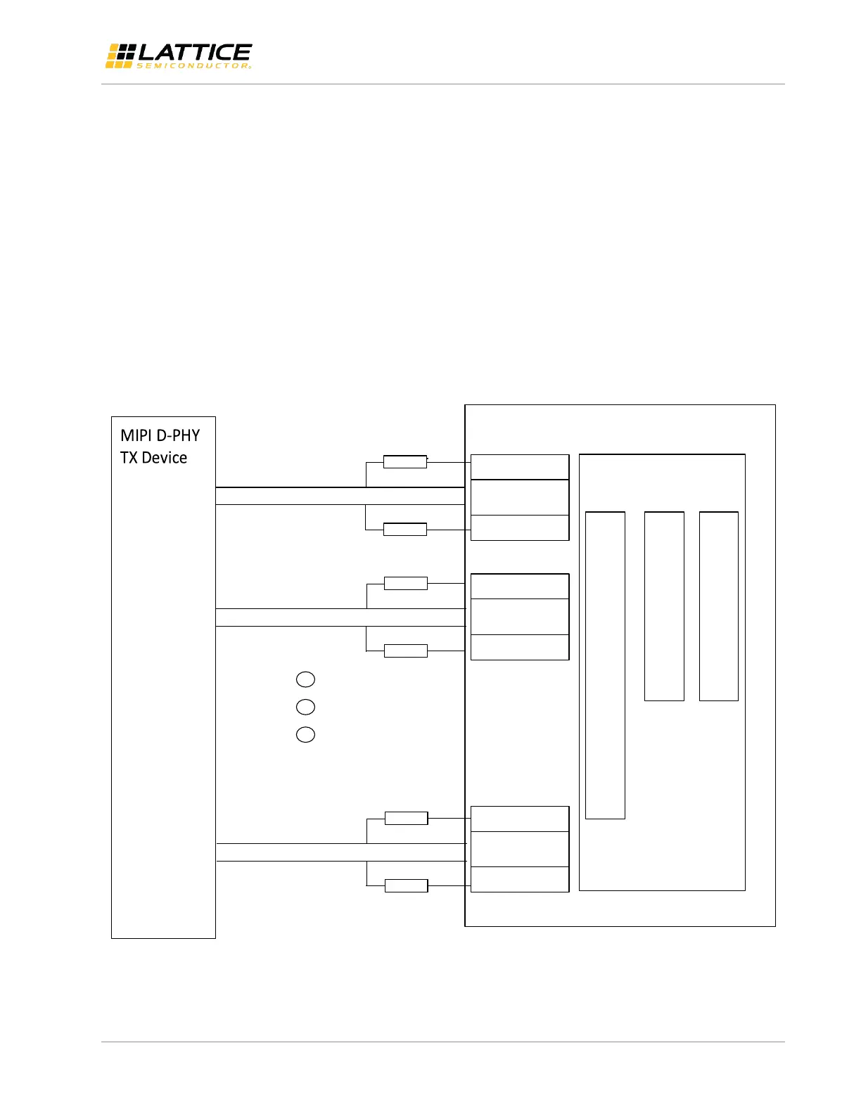
3. MIPI CSI-2/DSI Interfaces
MIPI Camera Serial Interface 2 (CSI-2) and Display serial Interface (DSI) are two of the serial interface protocols based
on MIPI D-PHY physical interface. MIPI D-PHY supports unidirectional HS (High Speed) mode and Bidirectional LP (Low
Power) mode. For the application of CMOS sensor bridge, we will only need the MIPI D-PHY receiver (RX) on the FPGA
receive interface, which allows the bridge to receive HS data on one clock lane and up to four data lanes. Figure 3.1
shows the block diagram of the Unidirectional Receive HS Mode and Bidirectional LP Mode interface. Figure 3.2 shows
the block diagram of the Unidirectional Receiver HS Mode Only interface. Figure 3.3 shows the block diagram of the
Unidirectional Transmit HS Mode and Bidirectional LP Mode interface. Figure 3.4 shows the block diagram of the
Unidirectional Transmit HS Mode Only interface.
Note: Figure 3.1 and Figure 3.2 do not apply to CrossLink since the CrossLink device uses dedicated MIPI D-PHY Input
buffers for both HS and LP mode to meet MIPI input voltage specfication. Figure 3.3 and Figure 3.4 also do not apply to
CrossLink as CrossLink’s programmable I/Os can only be configured as a MIPI D-PHY receiver (soft MIPI D-PHY). Only
the hardened MIPI D-PHY blocks can be configured as a transmitter.
For details on both Receiver/Transmitter HS and LP modes interface implementation, please refer to Lattice reference
design document MIPI D-PHY Interface IP (RD1182).
Aligner
iDDRx
4
I/O Controller
LVDS25
LVCMOS12
LVCMOS12
50 Ω
50 Ω
DATA3_P
DATA3_N
LP3[1]
D3_p
LP3[0]
D3_n
50 Ω
50 Ω
DATA0_P
DATA0_N
LP0[1]
D0_p
LP0[0]
D0_n
50 Ω
50 Ω
CLOCK_P
CLOCK_N
LPCLK[1]
DCK_p
LPCLK[0]
DCK_n
LVDS25
LVCMOS12
LVCMOS12
LVDS25
LVCMOS12
LVCMOS12
Figure 3.1. Unidirectional Receive HS Mode and Bidirectional LP Mode Interface Implementation
 Loading...