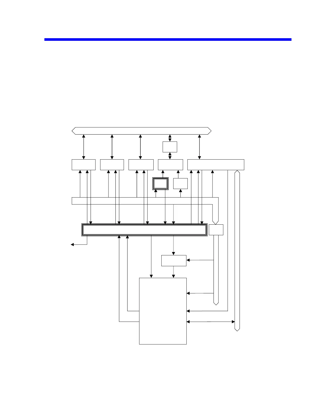
Relation of I/O Structure to the associated CPLDs
The following block-diagram describes the flow in the decoder and the relationships
between the acknowledgement to be returned to the CPU and CPLDs.
Three-line boxes are CPLDs, and one-line boxes indicate other ICs and function
blocks.
• SDM does all the controls for the access of the SDRAM (Initialize memory,
Decode and Mapping, Read/Write, Burst Read/Write, Refresh).
• Bus controls is the bus cycle of the entire CPU board. (Decode all areas other
than SDRAM, Read/Write of 32bits bus, Read/Write of the bus via bus sizer,
detection of bus error).
VG
Su
er MAIN SDRAM
MUX
CPU BUS
To CPU
Decoder
Buffe
Address
71059
GP-IB (16bit)
NVRAM
RTC
Small Peripherals
Front Panel
Flash ROM
PCMCIA (16bit)
CPU BUS (Data)
Buffe
BUS sizer
Figure 4-2 I/O Structure
Theory of Operation 4-9
 Loading...