Technical data
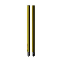
Leuze electronic MLC 520 Host/Guest 55
Weight see chapter 14.2 "Dimensions, weight, response
time"
Tab.14.4: System data - transmitter
Light source LED; exempt group in acc. with IEC62471
Wavelength 940 nm
Pulse duration 800 ns
Pulse pause 1.9µs (min.)
Mean power <50µW
Input current pin4 (range) Against +24V: 10mA
Against 0V: 10mA
Tab.14.5: System data receiver, indication signals and control signals
Pin Signal Type Electrical data
1 RES/STATE Input:
Output:
Against +24V: 15mA
Against 0V: 80mA
3 EDM Input: Against 0V: 15mA
4 RES Input: Against 24V: 15mA
Tab.14.6: Technical data of the electronic safety-related switching outputs (OSSDs) on the receiver
Safety-related PNP transistor outputs
(short-circuit monitored, cross-circuit
monitored)
Minimum Typical Maximum
Switching voltage high active (U
v
-1.5V) 18V 22.5V 27 V
Switching voltage low 0V +2.5V
Switching current 300mA 380mA
Residual current <2µA 200 µA
a)
Load capacity 0.3µF
Load inductivity 2H
Permissible wire resistance for load <200Ω
b)
Permissible wire cross section 0.25mm
2
Permissible cable length between receiver
and load
100m
Test pulse width 60μs 340μs
Test pulse distance (5ms) 60 ms
OSSD restart delay time after beam inter-
ruption
100ms
a) In the event of a failure (if the 0V cable is interrupted), each of the outputs behaves as a 120kΩ resistor
to U
v
. A downstream safety PLC must not detect this as a logical "1".
b) Note the additional restrictions due to cable length and load current.
NOTICE
The safety-related transistor outputs perform the spark extinction. With transistor outputs, it is
therefore neither necessary nor permitted to use the spark extinction circuits recommended by
contactor or valve manufacturers (RC elements, varistors or recovery diodes), since these con-
siderably extend the decay times of inductive switching elements.
 Loading...