EasyManua.ls Logo

LG CU920 - GSM Block Troubleshooting Steps

LG CU920
212 pages
To Next Page IconTo Next Page
To Previous Page IconTo Previous Page
Loading...
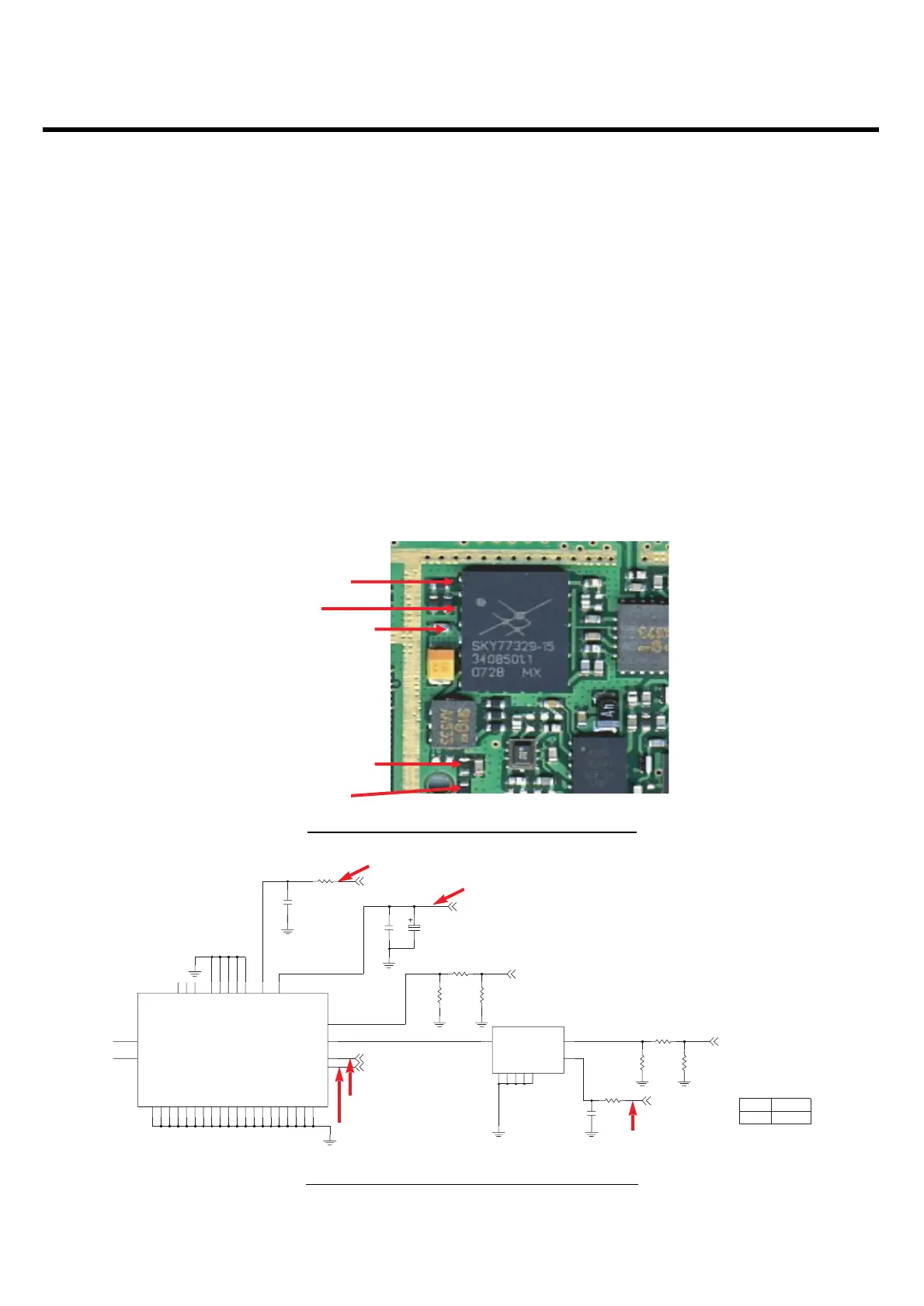
4.8.2 Checking PAM Block
1. TP1 : GSM_PA_RAMP
Power Amp Gain Control. typically, 0.2V < Vramp < 1.6V
2. TP2 : GSM_PA_EN
Power Amp Enable (Power ON : higher than 1.25V, Power OFF : lower than 0.4V)
3. TP3 : GSM_PA_BAND
Power Amp Band Selection Control
(GSM Mode : -0.2V < VBS < 0.4V, DCS/PCS Mode : 1.25V < VBS < 3.0V)
4. TP4 : +VPWR
PAM Supply Voltage Vcc higher than 3.0V
5. TP5 : GSM_SAW_SW_MODE
High : G900, Low : G850
LGE Internal Use Only
Copyright © 2008 LG Electronics. Inc. All right reserved.
Only for training and service purposes
4. TROUBLE SHOOTING
- 103 -
TP1
TP4
TP5
TP2
TP3
Fig. 4.8.2.1 Test point of the GSM PAM Block
7.75dB
HIGH
remain LOW when not transmitting
EGSM
GSM850
LOW
82
R115
51
R119
LMSM32AA-533
GND1
2
3
GND2
GND3
4
6
GND4
GND5
8
1
RFINRFOUT
5
7
VC
FL101
110
R120
C143
NA
200
R122
68p
C128
C132
33p
12
1
TX_EN
VAPC
6
5
VBATT
PGND15
PGND16
32
PGND17
33
34
PGND18
35
PGND19
PGND2
18
PGND20
36
19
PGND3
20
PGND4
PGND5
21
22
PGND6
23
PGND7
PGND8
24
PGND9
25
RSVD1
4
RSVD2
8
RSVD3
BS
2
DCS_PCS_IN
DCS_PCS_OUT
16
10
GND1
11
GND2
GND3
13
14
GND4
GND5
15
GSM_IN
7
GSM_OUT
9
PGND1
17
26
PGND10
27
PGND11
28
PGND12
PGND13
29
PGND14
30
31
U101
SKY77329
3
2.2KR113
33u
C129
R121
110
82
R116
R117
82
GSM_PA_EN
+VPWR
GSM_PA_RAMP
DCS_PCS_TX
GSM_PA_BAND
GSM_TX
GSM_SAW_SW_MODE
Fig. 4.8.2.2 Schematic of the GSM PAM Block
TP1
TP4
TP2
TP5
TP3

Other manuals for LG CU920

Related product manuals