16
PM3392A
CH1!10.0 V= MTB1.00ms ch1+
0V
+4V
-30V
PM3392A
CH1!2.00 V=
CH2 2 V= MTB10.0ms ch1+
+5V
0V
+5V
0V
I
2
C DATA
I
2
C CLK
PM3392A
CH1!10.0 V= MTB1.00ms ch1+
0V
+5V
-30V
Supply voltages
The display board receives several voltages via connector
JY01.
• VFTD : -30V ±5% measured at pin 2 of conn. JY01.
• VDC1-VDC2 : 4V3 ±10% measured between pin 1 and 3 of
conn. JY01.
• +5V : + 5V ±5% measured at pin 10 of conn. JY01.
Voltages VFTD, VDC1 and VDC2 are produced in the I/O Board
and sent to the display board via the CDR main board. The +5V
voltage is produced on the CDR main board as D5V.
Clock signal
As clock driver for the display controller, a resonator of 8 Mhz
(XY01) is used. The signal can be measured at pins 8 and 9 of
the display controller : 8 Mhz ±5%.
Control signals
RESETN
The reset signal comes via pin 4 of conn. JY01 from the DASP
master processor on the CDR main board (SYS_RESET). The
reset is low active. It should be kept low during power up for at
least 3 machine cycles with supply voltage in operating range
and a stable clock signal (1 machine cycle = 12 x 1/Fc (8 Mhz)
sec.). During normal operation, the reset should be high (3V3).
The high signal is 3V3 because the DASP operates on 3V3.
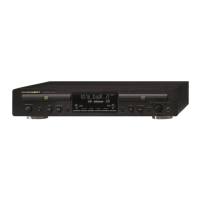
I2C DATA/I2C CLK
These lines connect to the DASP master processor via
respectively pin 5 and pin 7 of conn. JY01. When there is
no communication, they should have the high level (+5V). The
oscillogram below gives an indication of how these signals
should look like.
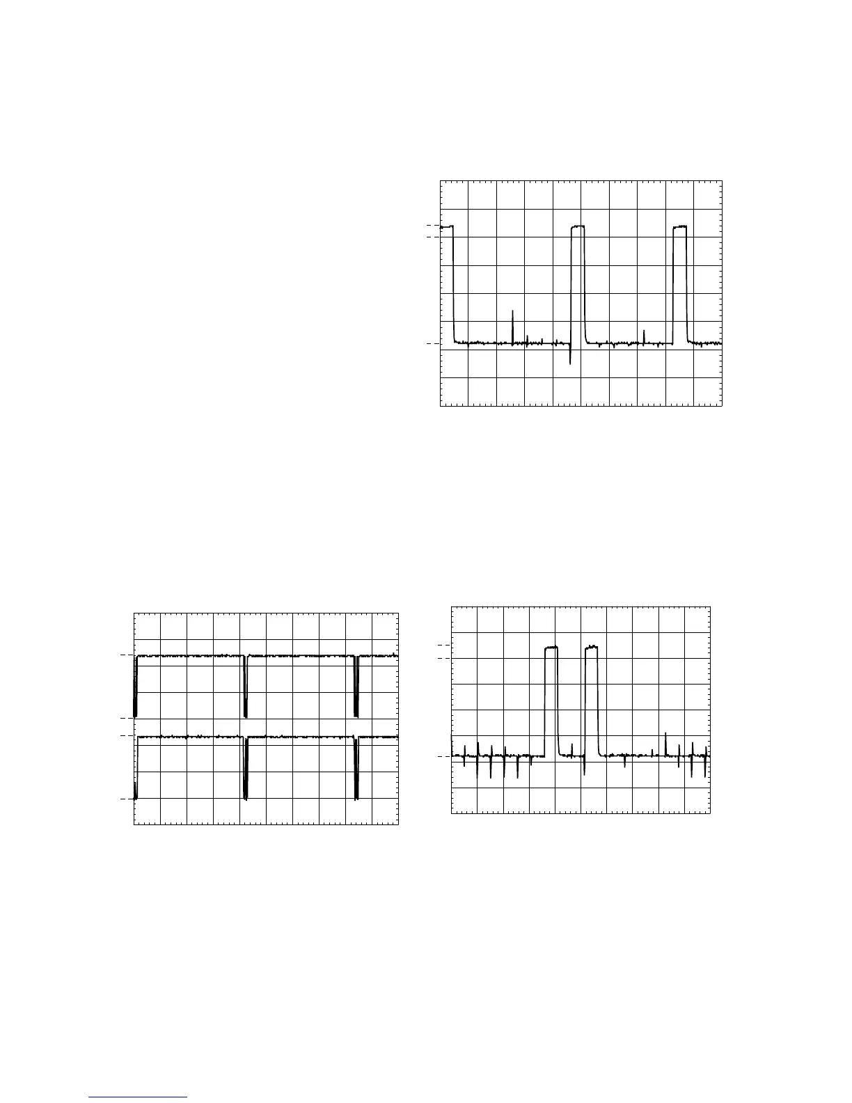
Grid lines
Level and timing of all grid lines, G1-->G15, can be checked
either at the FTD itself or at the display controller. Grid lines
G13, G14 and G15 each have an extra current amplifier in line
: QY04 for G13, QY03 for G14 and QY02 for G15. A typical
grid line signal shows in the oscillogram below.
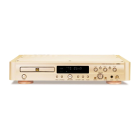
Segment lines
Level and timing of all segment lines, P-->P21, can be
checked either at the FTD itself or atthe display controller.
The data on these segment lines however, depends on the
characters displayed. The oscillogram below shows a
segment line with data. A segment line without data
maintains a -30V level.
FTD drive lines
Filament voltage
Should measure 4.3V ±10% (=VDC1-VDC2) between pins 1-2
and pins 52-53 of FTD(VY01).
7.1.2 Test instructions
Figure 7-2 “I2C SIGNALS”
Figure 7-3 “OSD”
Figure 7-4 “SEGMENT LINE”