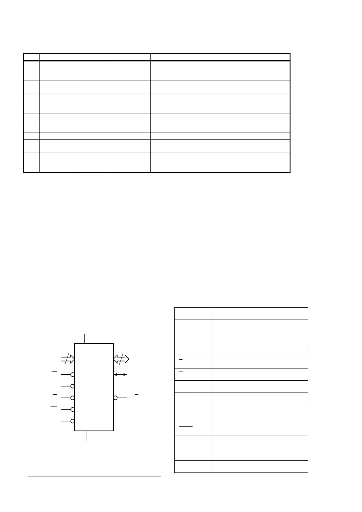
[PM01] QK01 : CM0039AF
No. Pin name I/O
3
Attribute Description
165 SCL IN
CMOS, Schmitt
3.3V Tolerant
Fail-Safe
MPU interface clock input pin.
166 VDDE P - VDD for IO (+ 3.3 V).
167 VSS P - Digital ground.
168 SLV IN CMOS
MPU interface slave address switch pin.
See Table 11-2.
169 N.C. OUT - Keep it open.
170 VSS P - Digital ground.
171 RFFI IN CMOS
MPEG information (repeat-first-field flag) input pin.
Connect it to the ground when not in use.
172 NRST IN CMOS, Schmitt System reset input pin (Low Active)
173 VDDE P - VDD for IO (+ 3.3 V).
174 VDDI P - VDD for Core (+ 1.8 V).
175 VSS P - Digital ground.
176 TPCP IN CMOS
Input pin exclusively for testing.
Connect it to the ground.
AI05470B
19
A0-A18
W
DQ0-DQ14
V
CC
M29W800DT
M29W800DB
E
V
SS
15
G
RP
DQ15A–1
RB
BYTE
A0-A18 Address Inputs
DQ0-DQ7 Data Inputs/Outputs
DQ8-DQ14 Data Inputs/Outputs
DQ15A–1 Data Input/Output or Address Input
E
Chip Enable
G
Output Enable
W
Write Enable
RP
Reset/Block Temporary Unprotect
RB
Ready/Busy Output
(not available on SO44 package)
BYTE
Byte/Word Organization Select
V
CC
Supply Voltage
V
SS
Ground
NC Not Connected Internally
[PM01] QJ50: M29W800DT70N1
178