169 170
2-18 2-18
2.5 IC DATA
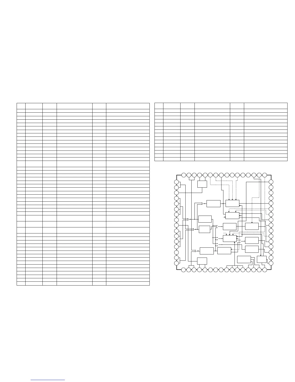
IC502 RH-iX1517GEZZ: RF Signal Processor (IX1517GE) (1/2)
1 GND Ñ GND terminal -
2 P2TP Input TE+ input (CD) VrA
3 P2TN Input TE- input (CD) VrA
4 LDO2 Output Drive output -
5 MDI2 Input Monitor output -
6 VrA Output Analog VREF 2.1 [V]
7 VrD Output Digital VREF - 1/2 of Vdd (2.1V)
8 VDD Input Power terminal Approx. 4.2V
9 DPAC - DPD AC coupling capacity 1 -
10 DPBD - DPD AC coupling capacity 2 --
11 DPD1 - DPD integration capacity 1 --
12 DPD2 - DPD integration capacity 2 -
13 SCB Input Control line (Bit clock) 2.2 [V]
14 SCL Input Control line (Latch signal) 2.2 [V]
15 SCD Input Control line (Serial data) 2.2 [V]
16 VRCK Input Reference clock input 2.3 [V] Frequency increase results in shift to
higher filter frequency except for servo LPF.
17 VCKF - Time constant adjustment capacity -
18 VCCP - Power terminal -
19 LVL Output Servo addition output VrD x (1/2)
20 TEO Output TE output VrD
21 FEO Output FE output VrD
22 DFTN Input DPD defect - DPD output at Low: Mute
23 VCCS - Power terminal (Servo) -
24 RPZ Output RF ripple center voltage VrD
25 RPO Output RF ripple output VrD
26 RPB Output RF ripple bottom -
27 RPP Output RF ripple peak -
28 RFO Output Equalizing RF output 2.3 [V]
29,30 NC - NC terminal - Used by connecting to GND.
31 VCCR - Power terminal (RF) -
32 DPDB Input Pit depth adjustment VrD DPDB increase brings delay capacity
increase on sides A and B.
33 TEB Input TE balance VrD TEB increase brings increase in gain on TP
side and in delay capacity on sides A and C.
34 FEB Input FE balance VrD FEB increase brings increase in gain on
sides A and C (FP).
35 PSC Input VRCK frequency division ON/OFF - Frequency division OFF at High
36 VCC2 - Power terminal -
37 NC - NC terminal VrD Connected to GND via C.
38 EQD Input Group delay correction VrD Group delay by raising EQD: rise rightward
39 GND2 - GND terminal -
40 RFDC - DC feedback capacity -
41* RFA Output RF total adding output 2.2 [V]
42 EQB Input Boost adjustment VrD Boost quantity up by raising EQB.
43 EQF Input Frequency adjustment VrD Shift to higher frequency by raising EQF.
44 MDI1 Input Monitor input -
45 LDO1 Output Drive output -
46 P1TN Input TE- input (DVD) VrA
47 P1TP Input TE+ input (DVD) VrA
48 NC - NC terminal - Used by connecting to GND.
49
P1FN
Input FE- input (DVD) VrA
Pin No. Terminal Name
Input/Output
Function
Terminal DC
Voltage (TYP.)
Remarks
In this unit, the terminal with asterisk mark (*) is (open) terminal which is not connected to the outside.
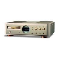
IC502 RH-iX1517GEZZ: RF Signal Processor (IX1517GE) (2/2)
50 P1FP Input FE+ input VrA
51 LDP1 Input APC polarity 1 - Positive polarity when connecting to Vcc
52 P1DI Input D input (DVD) VrA
53 P1CI Input C input (DVD) VrA
54 P1BI Input B input (DVD) VrA
55 P1AI Input A input (DVD) VrA
56 GNDR - GND terminal (RF) -
57 LDP2 Input APC polarity 2 - Positive polarity when connecting to Vcc
58 P2AI Input A input (CD) VrA
59 P2BI Input B input (CD) VrA
60 P2CI Input C input (CD) VrA
61 P2DI Input D input (CD) VrA
62 GNDS - GND terminal (Servo) -
63 P2FP Input FE+ input VrA
64 P2FN Input FE- input VrA
Pin No. Terminal Name
Input/Output
Function
Terminal DC
Voltage (TYP.)
Remarks
P1FN
P1FP
LDP1
P1DI
P1CI
P1BI
P1AI
GNDR
LDP2
P2AI
P2BI
P2CI
P2DI
GNDS
P2FP
P2FN
DPDB
VccR
NC
NC
RFO
RPP
RPB
RPO
RPZ
VccS
DFTN
FEO
TEO
LVL
LccP
VCKF
NC
P1TP
P1TN
LDO1
MDI1
EQF
EQB
RFA
RFDC
GND2
EQD
NC
Vcc2
PSC
FEB
TEB
GND
P2TP
P2TN
LDO2
MDI2
VrA
VrD
Vdd
DPAC
DPBD
DPD1
DPD2
SCB
SCL
SCD
SRCK
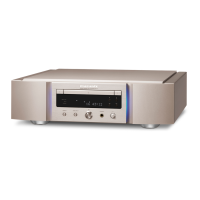
12345678910111213141516
17
18
19
20
21
22
23
24
25
26
27
28
29
30
31
32
48 47 46 45 44 43 42 41 40 39 38 37 36 35 34 33
64
63
62
61
60
59
58
57
56
55
54
53
52
51
50
49
APC1
sel-RF
R-gain
ADJUSTMENT
EQ
F-gain
ADJUSTMENT
F-gain
ADJUSTMENT
RF RIPPLE
GENERATION
FE
GENERATION
DPDTE
GENERATION
FE-gain
ADJUSTMENT
TE-gain
ADJUSTMENT
Level
DETECTION
T-gain
ADJUSTMENT
3BTE
GENERATION
APC2
BUS
sel-PD
sel-PD
sel-PD
mode-TE
sel-FE
sel-IC
sel-TE
sel-DPD
sel-LVL
Time
constant
adjustment