2-19 2-20
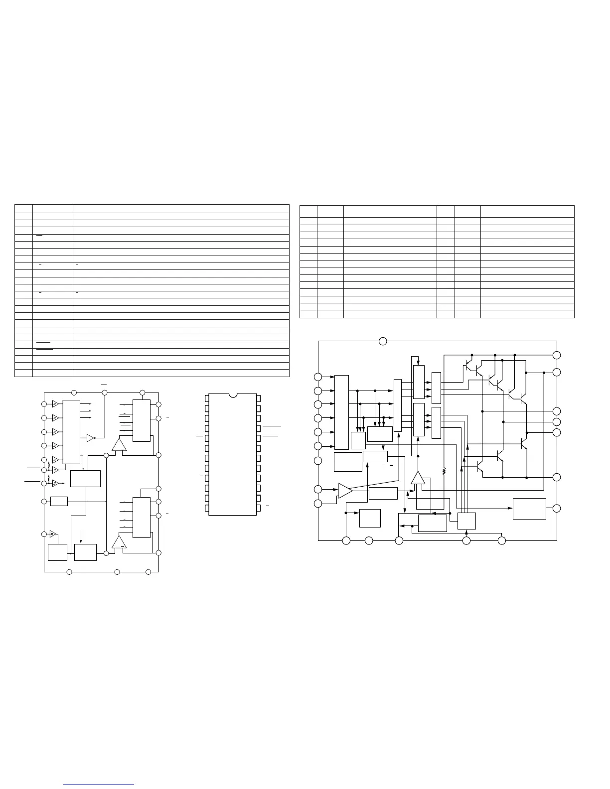
IC503 VHiTB6504F+-1: Stepping Motor Driver (TB6504F)
1 CK1 Clock signal input
2, 3 M1, M2 Excitation mode set terminal
4 REF IN Output reference value (VNF) set terminal H: VNF=0.5V, L: VNF=0.25V
5* MO Monitor output L: Initial condition
6* NC Not used
7 VCC Logic side power terminal
8 VMB Output side power terminal
9 øB B output
10 PG-B Power ground
11 NFB B channel current detection terminal
12 øB B output
13 øA A output
14* NFA A channel current detection terminal
15 PG-A Power ground
16 øA A output
17 VMA Output side power terminal
18* NC Not used
19 S-GND Signal ground
20 RESET Reset signal input
21 ENABLE Enable signal input
22 OSC Internal oscillation frequency set terminal. Capacitor is externally mounted.
23 CW/CCW Clockwise/counterclockwise input
24 CK2 Clock signal input
Pin No. Terminal Name
In this unit, the terminal with asterisk mark (*) is (open) terminal which is not connected to the outside.
Function
7
VCC
5
MO
17
16
13
YMA
¯A
¯A IA
14
NFA
8
VMB
12
9
¯B
11
10
NFB
¯B IB
PG-B
(POWER
GROUND B)
15
PG-A
(POWER
GROUND A)
19
4
SG
(SIGNAL GROUND)
REF IN
22
OSC
21
ENABLE
20
RESET
24
CK2
23
CW/CCW
1
CK1
3
M2
2
M1
O S C
+
+
+
+
BRIDGE
DRIVER
ENABLE
RESET
BRIDGE
DRIVER
ENABLE
RESET
DECODER
DECODER
DECODER
DECODER
SET CURRENT
VALUE SELECTOR
CIRCUIT
SET CURRENT
VALUE SELECTOR
CIRCUIT
MAXIMUM
CURRENT
SELECTOR
CIRCUIT
CK1
M1
M2
REF IN
MO
NC
VCC
VMB
¯B
PG-B
NFB
¯B
CK2
CW/CCW
OSC
ENABLE
RESET
S-GND
NC
VMA
¯A
PG-A
NFA
¯A
1
2
3
4
5
6
7
8
9
10
11
12
24
23
22
21
20
19
18
17
16
15
14
13
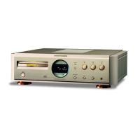
IC504 RH-iX2842AFZZ: Spindle Motor Driver (IX2842AF)
In this unit, the terminal with asterisk mark (*) is (open) terminal which is not connected to the outside.
Pin No.
Terminal
Name
Function Pin No.
Terminal
Name
Function
1 PG Power GND terminal 15 SG Signal GND terminal
2 H1+ Hall element 1 positive input terminal 16 VCC Power terminal
3 H1- Hall element 1 negative input terminal 17 ECR Torque instruction reference input terminal
4* NC Not used 18 EC Torque instruction input terminal
5 H2+ Hall element 2 positive input terminal 19* NC Not used
6 H2- Hall element 2 negative input terminal 20 PCI
Current feedback phase compensating terminal
7 VH Hall bias terminal 21 VM Motor power terminal
8 H3+ Hall element 3 positive input terminal 22 CS1 Current detection terminal 1
9 H3- Hall element 3 negative input terminal 23* NC Not used
10 SS Start/Stop switching terminal 24* NC Not used
11* TFLG Thermal protection monitor terminal 25* NC Not used
12 FG FG signal output terminal 26 A3 Drive output 3
13 BRK Break mode set terminal 27 A2 Drive output 2
14* NC Not used 28 A1 Drive output 1
2
H1+
3
H1-
5
H2+
8
H3+
6
H2-
9
H3-
7
VH
18
EC
17
10
ECR
S/S
16
Vcc
20
PCI
13
BRK
11
TSDF
12
FG
1
PG
26
A3
27
A2
28
A1
22
CS1
21
VM
15
SG
ER
EA
VTL
EP=ER x EA
FG
COMPARATOR
+ -
MATRIX HALL AMPLIFIER
DETE-
CTION
DIRECTION
DETECTION
DIRECTION SWITCHING
UPPER-SIDE
DISTRIBUTION
AMPLIFICATION
AMPLIFICATION
LOWER-SIDE
DISTRIBUTION
HALL BIAS
LOGIC
ABSOLUTE
VALUE
START/
STOP
THERMAL
PROTECTION
CIRCUIT
BREAK
CIRCUIT