2-21 2-22
CTL1 CTL2 CH1 CH2 CH3 CH4 CH5
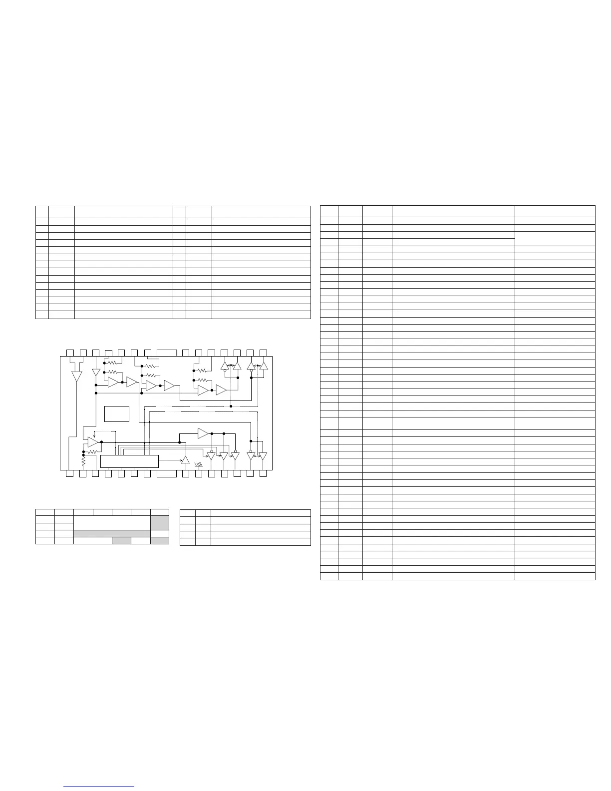
IC506 VHiBA6796FP-1: Loading/Focus/Tracking/Spin/Sled Driver (BA6796FP)
Note 1: Positive output/negative output means polarity toward input. (Ex. 18 pin output 'H' in case of 19 pin input 'H')
Note 2: Tray positive output/tray negative output means polarity toward mode. (Ex. 11 pin output 'H' in case of the forward mode)
In this unit, the terminal with asterisk mark (*) is (open) terminal which is not connected to the outside.
Pin
No.
Terminal
Name
Function
Pin
No.
Terminal
Name
Function
1* OPOUT Operational amplifier output terminal 15 CH2-OUT- CH2 negative output terminal
2 CH4-IN CH4 input terminal 16 CH2-OUT+ CH2 positive output terminal
3* CH4-IN' CH4 gain adjustment input terminal 17 CH1-OUT- CH1 negative output terminal
4 CTL1 Control 1 input terminal 18 CH1-OUT+ CH1 positive output terminal
5 CTL2 Control 2 input terminal 19 CH1-IN CH1 input terminal
6 FWD Tray forward input terminal 20 CH1-IN'
CH1 gain adjustment input terminal
7 REV Tray reverse input terminal 21 VCC VCC
8 TRAY-IN Tray input terminal 22 CH2-IN CH2 input terminal
9 GND Substrate GND 23* CH2-IN'
CH2 gain adjustment input terminal
10 CH5-OUT- Tray negative output terminal 24* CH3-IN CH3 input terminal
11 COM-OUT
Tray positive terminal/CH4 negative output terminal
25* CH3-IN'
CH3 gain adjustment input terminal
12* CH4-OUT+ CH4 positive output terminal 26 VREF-IN Bias amplifier input terminal
13* CH3-OUT+ CH3 positive output terminal 27* OPIN+
Operational amplifier non-inversion input terminal
14* CH3-OUT- CH3 negative output terminal 28* OPIN- Operational amplifier inversion input terminal
28 27 26
25
24 23 22 21 20 19 18 17 16 15
CH2-OUTCH1-OUTCH1-INCH2-INCH3-IN
10K
10K
13.3K
13.3K
13.3K
10K
+
-
VCC
DDDD
DDDDD
V/I
T.S.D
26.6K
10K
CTL1 CTL2 PWD REV
LOGIC
1234567 891011121314
CH4-IN CH5-IN CH5-OUT CH4-OUT CH3-OUT
+
-
+
-
+
-
+-
LEVEL SHIFT
LEVEL SHIFT
LEVEL SHIFT
LEVEL SHIFT
Mode Switching Table
For CTL1 and CTL2
LL
OFF ON
LH
H L ON OFF
H H OFF ON OFF ON
Note: Output: high impedance in case of OFF.
For F and R (CH5 control is effective only in case of ON)
F R Output Mode
L L High impedance
L H Reverse
H L Forward
H H Break
IC602 RH-iX1474GEZZ: SACD Data Processor (IX1474GE) (1/2)
1 DPCKI Input Signal processing reference clock input 0.5 - 3.3Vpp, feedback resistor built in.
2 DVDD3 - Digital power supply (3.3V) For logic cell
3 SVCKI Input Servo reference clock input (Oscillation circuit input terminal) 3.3V-I/F feedback resistor built in
4* SVCKO Output Servo reference clock input (Oscillation circuit input terminal)
5 DVSS - Digital power supply (0V) For logic cell
6 DVDD3 - Digital power supply (3.3V) For logic cell
7* NC - The use forbidden Open
8 HDWT Input MPU write signal Level TTL
9 HDRD Input MPU read signal Level TTL
10 HCEN Input MPU chip select Level TTL
11-18 HD0-HD7 Input/Output MPU data bus Level TTL
19 DVSS - Digital power supply (0V) For I/O cell
20 DVDD5 - Digital power supply (5V) For I/O cell
21 HINT Output MPU interrupt signal (Occurrence of interruption = "L") OPEN DRAIN
22,23 HA0, HA1 Input MPU address bus Level TTL
24 PLCK Output Read channel clock output terminal
25*-31* ED0-ED6 - For default adjustment; use by user is forbidden. (NC) Open
32 ED7 Output SACD 2 binary data
33 TEST Input For default adjustment Set to "L".
34 PDON Output PLL phase error signal output (Polarity: -)
35 PDOP Output PLL phase error signal output (Polarity: +)
36 RLLD Output PLL detection result output
37 LPFN Input Inversion input of amplifier for PLL loop filter
38 LPFO Output Output of amplifier for PLL loop filter
39 VCOF Output VCO filter terminal
40 SCLO Output Reference voltage output terminal of built-in comparator
41 AVSS - Analog power supply (0V)
42 AVR Output Non-PLL analog reference potential (1.65V)
43 VRC - Resistance dividing point potential
(For generating analog reference potential: 1.65)
44 PVR Output PLL analog reference potential (1.65V)
45 AVDD - Analog power supply (3.3V)
46 RVR2 - Secondary reference voltage (For connecting capacitor)
47 RVDD - Dedicated power terminal (3.3V)
48 RFIN Input RF signal input
49 RVSS - Dedicated power terminal (0V)
50 RVR1 - The first reference voltage (For connecting capacitor)
51 DVR Input DMO reference potential (1.65V recommended)
52 DMO Output DVD disc equalizer output (Ternary PWM + Hiz)
53 RASN Output External RAM column address select (Negative logic)
54 CASN Output External RAM row address select (Negative logic)
55 MOEN Output External RAM output enable signal
56 MWEN Output External RAM read/ write select
57 DVSS - Digital power supply (0V) For logic cell
58 DVDD3 -- Digital power supply (3.3V) For logic cell
59-68 MA9-MA0 Output External RAM address bus
69 DVSS - Digital power supply (0V) For I/O cell
70 DVDD5 - Digital power supply (5V) For I/O cell
71-78 MD7-MD0 Input/Output External RAM data bus Level TTL
79-82 SD7-SD4 Output MPEG data output
83
DVSS
- Digital power supply (0V) For logic cell
Pin No.
Terminal
Name
Input/Output Function
Remarks
In this unit, the terminal with asterisk mark (*) is (open) terminal which is not connected to the outside.
 Loading...