2-33 2-34
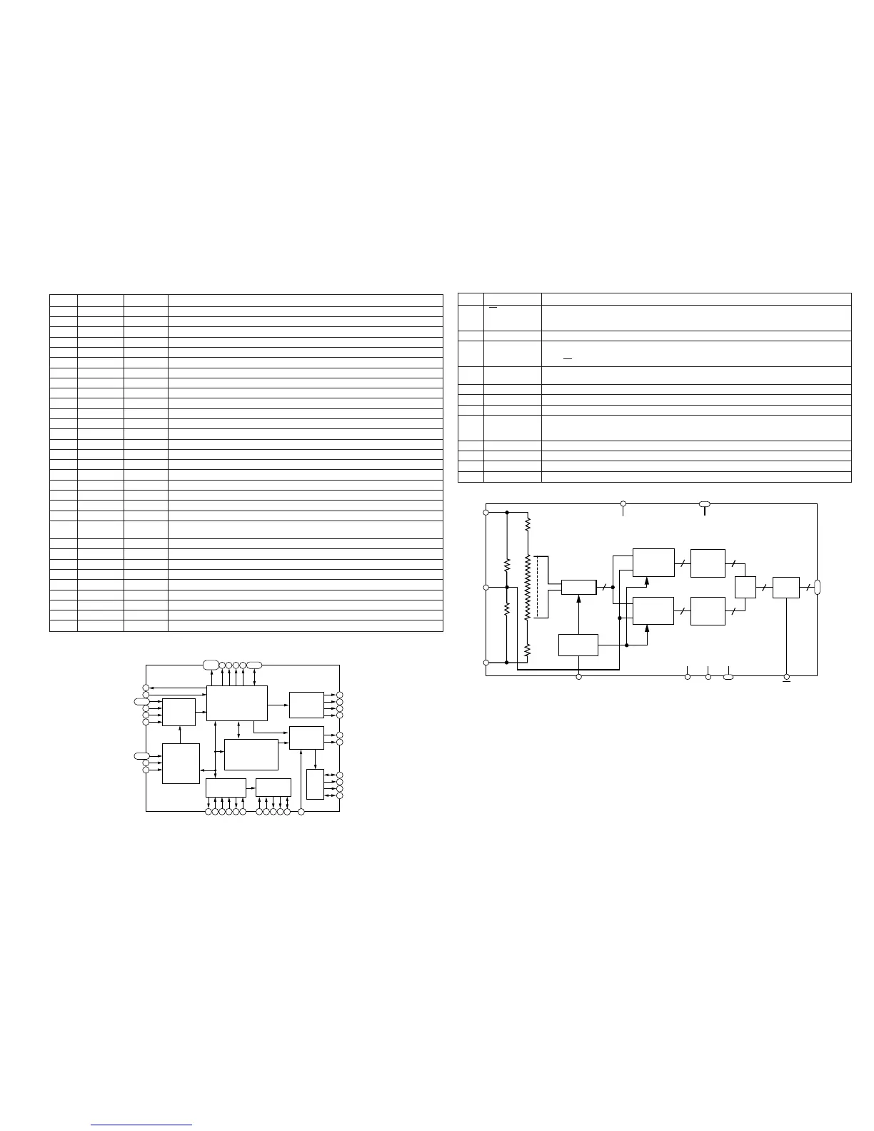
IC901 VHiCXD2751Q-1: SACD Playback Signal Processor (CXD2751Q) (2/2)
46 BCKA Input/Output Shift clock input/output terminal for DSD data output. Input/output according to setting.
47 DSAL Output Lch-DSD data output terminal. Phase modulation output according to setting.
48 DSAR Output Rch-DSD data output terminal. Phase modulation output according to setting.
49 ZDFLGL Output Lch zero data detection flag. "H": when silent data continue for 300msec.
50 ZDFLGR Output Rch zero data detection flag. "H": when silent data continue for 300msec.
51 A0 Output DRAM address output terminal (LSB)
52 A1 Output DRAM address output terminal
53 VDD - Power supply terminal, +3.3V
54 VSS - Ground terminal
55-62 A2-A9 Output DRAM address output terminal
63 A10 Output DRAM address output terminal (MSB)
64* NC - Not used
65 VSS - Ground terminal
66 XWE Output DRAM write enable output terminal. Connected to WE terminal of DRAM.
67 XCAS Output DRAM column address strobe output terminal. Connected to CAS terminal of DRAM.
68 XRAS Output DRAM row address strobe output terminal. Connected RAS terminal of DRAM.
69 XOE Output DRAM read enable output terminal. Connected OE terminal of DRAM.
70-77 DQ0-DQ7 Input/Output DRAM data input/output terminal
78 VDD - Power supply terminal, +3.3V
79 VSS - Ground terminal
80 WCK Input Operation clock for detecting PSP physical disc mark. Inputs 27.00MHz.
81 WRFD Input RF data input terminal for detecting PSP physical disc mark
Inputs RF data made binary by slicer.
82 WAD0 Input A/D data input/output terminal for detecting PSP physical disc mark (LSB)
83-88 WAD1-WAD6 Input A/D data input/output terminal for detecting PSP physical disc mark
89 WAD7 Input A/D data input/output terminal for detecting PSP physical disc mark (MSB)
90 VSS - Ground terminal
91 SD7 Input Input terminal for stream data to be output from the front end processor (MSB)
92-97 SD6-SD1 Input Input terminal for stream data to be output from the front end processor
98 SD0 Input Input terminal for stream data to be output from the front end processor (LSB)
99 SDEF Input Input terminal for error flag to be output from the front end processor
100 XSAK Input Input terminal for data effective flag to be output from the front end processor
Pin No.
Terminal Name
Input/Output
Function
In this unit, the terminal with asterisk mark (*) is (open) terminal which is not connected to the outside.
1
99
91 ~ 98
89 ~ 82
5
2
81
80
11 7 8 9 10 13 14 16 17 18
19 6
42
48
47
46
50
49
33
36
35
34
69666768
77 ~ 70
100
63~55,
52, 51
PSP
CPU-I/F
DSD
I/F
SUP-I/F
FADE-
INPUT/OUTPUT
XSRQ
SDEF
SD[7:0]
WAD[7:0]
SDCK
XSAK
XSHD
WRFD
WCK
MSREDY
XMSLAT
MSCK
MSDATI
MSDATO
XRST
MCKI
CK75S
EXCKO1
EXCKO2
LRCK
SMUTE
BCKA
DSAL
DSAR
BCKD
SUPDAT
XSUPAK
SUPEN
F75HZ
A[10:0]
XRAS
XCAS
XWE
XOE
DQ[7:0]
DECRYPTION
STREAM MANAGER
DIRECT STREAM
TRANSFER DECODER
TIMING
IC902 VHiADC08351-1: A/D Converter (ADC08351)
1 OE CMOS/TTL compatible digital input terminal.
When this terminal is set to Low, digital output of ADC08351 becomes enable.
When this terminal is set to High, digital output changes to the high-impedance condition.
2 DGND Ground return circuit terminal for digital power supply.
3-10 D0-D7 Conversion data output terminal. C0 shows LSB, and D7 shows MBS.
Effective data are output on data bus immediately after CLK input rising edge.
When OE terminal is set to Low, these terminals become enable.
11 VD Positive digital power voltage terminal. Connected to +3V power supply.
VA and VD are supplied from the common power supply.
12 CLK CMOS/TTL compatible clock input terminal. VIN is sampled at CLK input trailing edge.
13 VD Positive digital power voltage terminal. Connected to +3V voltage power.
14 VREF Positive reference voltage input terminal. Voltage of this terminal ranges from 0.75V to VA.
15 PD CMOS/TTL compatible digital input terminal.
When this terminal is set to High, ADC08351 enters the power down mode, minimizing power consumption.
When this is set to Low, the device enters the normal operation mode.
16 VA Positive analog power voltage terminal: To connect +3V voltage power.
17 VIN Analog signal input. Convertible input ranges from 0.5Vp-p to 0.68Va.
18, 19 AGND Ground return circuit terminal for analog power supply.
20 DGND Ground return circuit terminal for digital power supply.
Pin No. Terminal Name Function
 Loading...