44
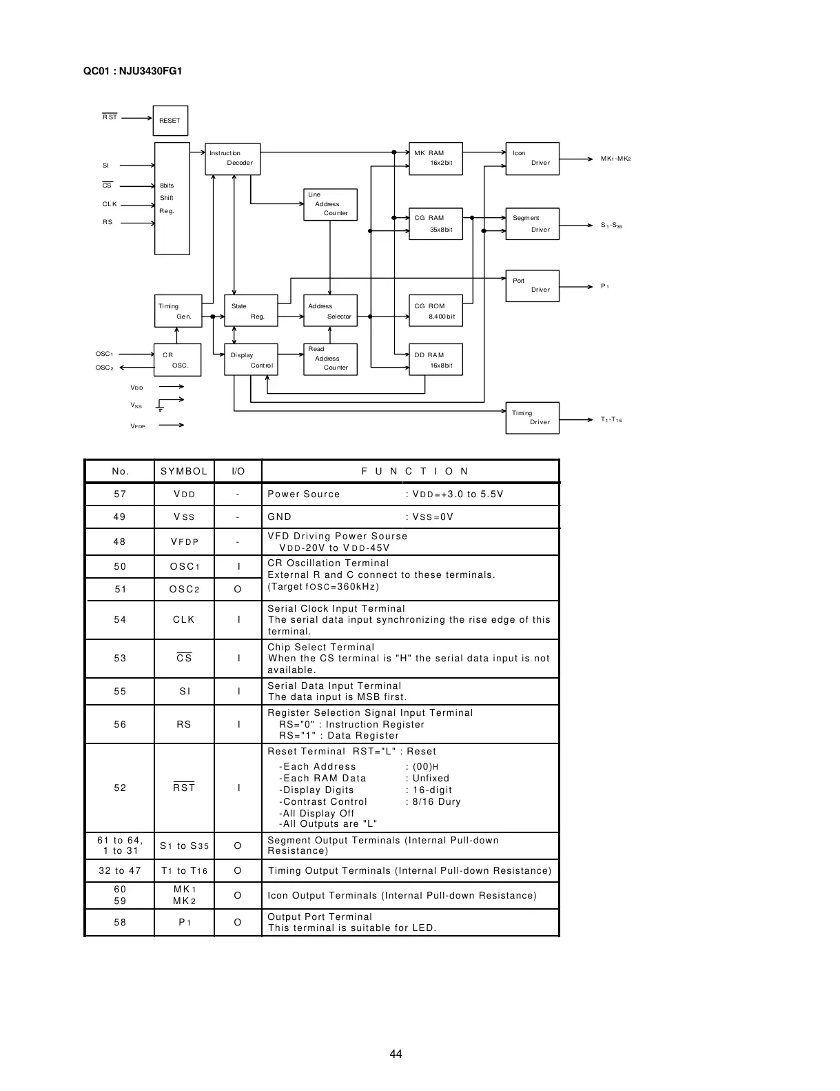
No. SYMBOL I/O F U N C T I O N
57 VDD - Power Source : VDD=+3.0 to 5.5V
49 VSS - GND : VSS=0V
48 VFDP -
VFD Driving Power Sourse
V
DD-20V to VDD-45V
50 OSC1 I
CR Oscillation Terminal
External R and C connect to these terminals.
(Target f
OSC=360kHz)
51 OSC2 O
54 CLK I
Serial Clock Input Terminal
The serial data input synchronizing the rise edge of this
terminal.
53 CS I
Chip Select Terminal
When the CS terminal is "H" the serial data input is not
available.
55 SI I
Serial Data Input Terminal
The data input is MSB first.
56 RS I
Register Selection Signal Input Terminal
RS="0" : Instruction Register
RS="1" : Data Register
52 RST I
Reset Terminal RST="L" : Reset
-Each Address
-Each RAM Data
-Display Digits
-Contrast Control
-All Display Off
-All Outputs are "L"
: (00)
H
: Unfixed
: 16-digit
: 8/16 Dury
61 to 64,
1 to 31
S
1 to S35 O
Segment Output Terminals (Internal Pull-down
Resistance)
32 to 47 T1 to T16 O Timing Output Terminals (Internal Pull-down Resistance)
60
59
MK1
MK2
O Icon Output Terminals (Internal Pull-down Resistance)
58 P1 O
Output Port Terminal
This terminal is suitable for LED.
SI
CS
CLK
RS
V
SS
OSC
1
OSC
2
V
DD
RST
V
FDP
MK
1
~
MK
2
S
1
~
S
35
P
1
T
1
~
T
16
8bits
Shift
Reg.
Instruction
Decoder
Timing
Gen.
CR
OSC.
State
Reg.
Display
Cont rol
Address
Selector
Read
Address
Counter
Li ne
Address
Counter
Timing
Driver
DD RAM
16x8 bit
CG ROM
8,400bit
Port
Driver
CG RAM
35x8 bit
Segment
Driver
MK RAM
16x2 bit
Icon
Driver
RESET
QC01 : NJU3430FG1