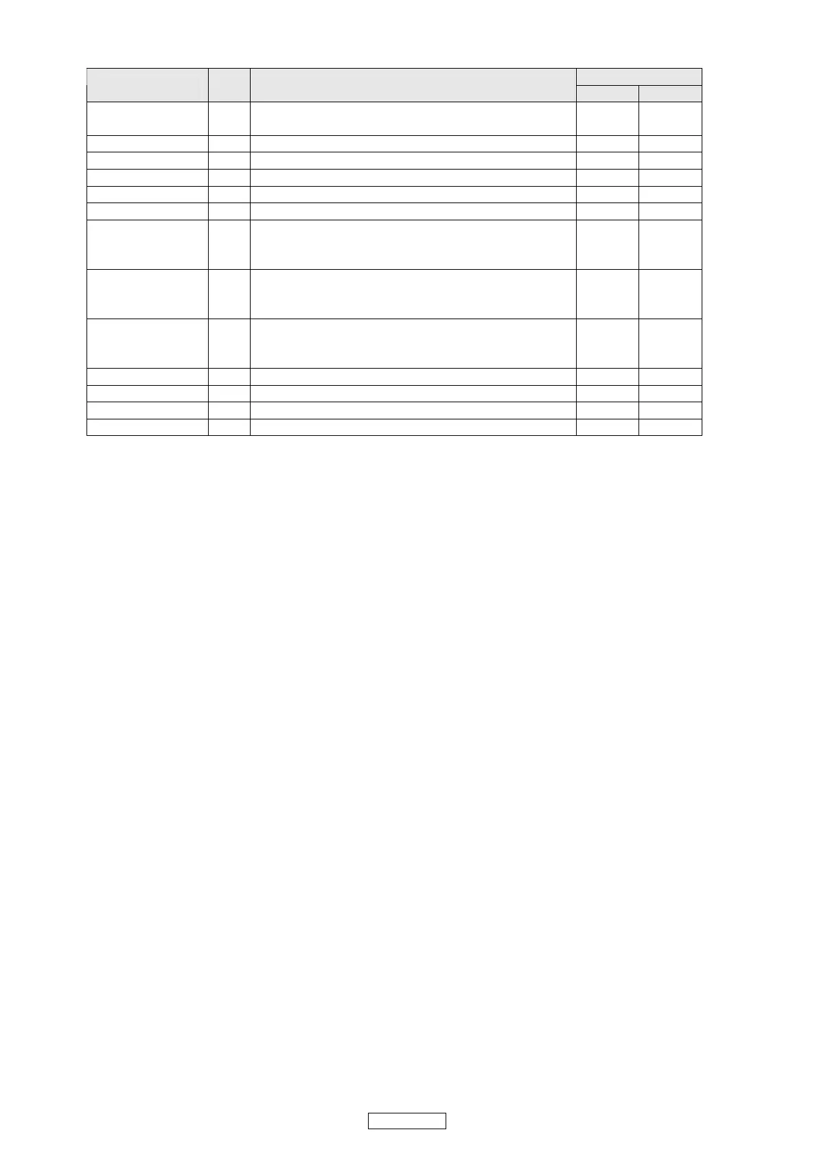
59
UD9004
PT6302-R-001(L) Pin Function
Pin No.
Pin Name I/O Description
LQFP SSOP
SG5 to SG35
SG4 to SG1
O Segment driver output pin
1 ~ 31
64 ~ 61
9 ~ 39
8 ~ 5
GR1 to GR16 O Grid driver output pin 32 ~ 47 40 ~ 55
VEE - Power supply 48 56
VSS - Ground pin 49 57
OSCI I Oscillator input pin 50 58
OSCO O Oscillator output pin 51 59
RSTB I
Reset input pin
When this pin is set to "LOW", all functions are
initialized.
52 60
CSB I
Chip select input pin
When this pin is set to "High" Level, the serial data
transfer is disabled.
53 61
CLKB I
Shift clock input pin
The serial data is shifted at the rising edge of
CLKB.
54 62
DIN I Serial data input pin 55 63
VDD - Positive power supply 56 64
P1 to P2 O General purpose output pin 57 ~ 58 1 ~ 2
AD2 to AD1 O Segment driver output pin 59 ~ 60 3 ~ 4