65
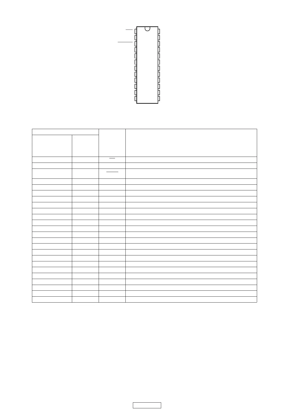
UD9004
PCA9539PW,188 (8U-310002 : IC102)
PCA9539PW,188 Pin Function
INT
A1
RESET
P00
P01
P02
P03
P04
P05
P06
P07
GND
V
CC
SDA
SCL
A0
P17
P16
P15
P14
P13
P12
P11
P10
24
23
22
21
20
19
18
17
16
15
14
13
1
2
3
4
5
6
7
8
9
10
11
12
NO.
SOIC (DW),
SSOP (DB),
NAME DESCRIPTION
QSOP (DBQ), QFN (RGE)
TSSOP (PW), AND
TVSOP (DGV)
1 22 INT
Interrupt output. Connect to V
CC
through a pullup resistor.
2 23 A1 Address input. Connect directly to V
CC
or ground.
Active-low reset input. Connect to V
CC
through a pullup resistor if no active
3 24 RESET
connection is used.
4 1 P00 P-port input/output. Push-pull design structure.
5 2 P01 P-port input/output. Push-pull design structure.
6 3 P02 P-port input/output. Push-pull design structure.
7 4 P03 P-port input/output. Push-pull design structure.
8 5 P04 P-port input/output. Push-pull design structure.
9 6 P05 P-port input/output. Push-pull design structure.
10 7 P06 P-port input/output. Push-pull design structure.
11 8 P07 P-port input/output. Push-pull design structure.
12 9 GND Ground
13 10 P10 P-port input/output. Push-pull design structure.
14 11 P11 P-port input/output. Push-pull design structure.
15 12 P12 P-port input/output. Push-pull design structure.
16 13 P13 P-port input/output. Push-pull design structure.
17 14 P14 P-port input/output. Push-pull design structure.
18 15 P15 P-port input/output. Push-pull design structure.
19 16 P16 P-port input/output. Push-pull design structure.
20 17 P17 P-port input/output. Push-pull design structure.
21 18 A0 Address input. Connect directly to V
CC
or ground.
22 19 SCL Serial clock bus. Connect to V
CC
through a pullup resistor.
23 20 SDA Serial data bus. Connect to V
CC
through a pullup resistor.
24 21 V
CC
Supply voltage