Doc. No. MV-S105540-00, Rev. A
Page 14 Document Classification: Proprietary Information
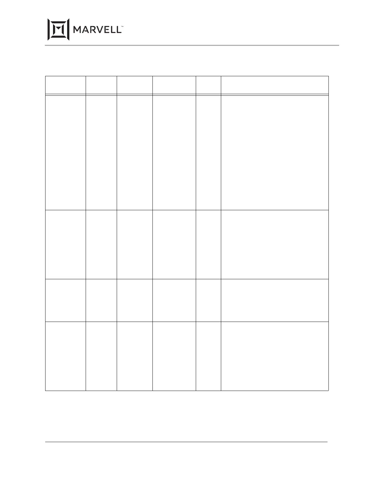
J2
J1
H3
H1
H2
G3
G2
F1
B10
A10
B9
A9
B8
B7
B6
A6
29
28
26
25
24
20
19
18
TXD[7]
TXD[6]
TXD[5]
TXD[4]
TXD[3]/TXD[3]
TXD[2]/TXD[2]
TXD[1]/TXD[1]
TXD[0]/TXD[0]
I GMII and MII Transmit Data. In GMII mode,
TXD[7:0] present the data byte to be trans-
mitted onto the cable in 1000BASE-T mode.
In MII mode, TXD[3:0] present the data nib-
ble to be transmitted onto the cable in
100BASE-TX and 10BASE-T modes.
TXD[7:4] are ignored in these modes, but
should be driven either high or low. These
pins must not float.
TXD[7:0] are synchronous to GTX_CLK, and
synchronous to TX_CLK in 100BASE-TX
and 10BASE-T modes.
Inputs TXD[7:4] should be tied low if not
used (e.g., RGMII mode).
C1 B1 7 RX_CLK O, Z GMII and MII Receive Clock. RX_CLK pro-
vides a 125 MHz clock reference for RX_DV,
RX_ER, and RXD[7:0] in 1000BASE-T
mode, a 25 MHz clock reference in
100BASE-TX mode, and a 2.5 MHz clock
reference in 10BASE-T mode.
TX_TCLK comes from the RX_CLK pins
used in jitter testing. Refer to Register 9 for
jitter test modes.
B1 B44 4 RX_DV O, Z GMII and MII Receive Data Valid. When
RX_DV is asserted, data received on the
cable is decoded and presented on
RXD[7:0] and RX_ER.
RX_DV is synchronous to RX_CLK.
D2 A2 8 RX_ER O, Z GMII and MII Receive Error. When RX_ER
and RX_DV are both asserted, the signals
indicate an error symbol is detected on the
cable.
When RX_ER is asserted with RX_DV de-
asserted, a false carrier or carrier extension
symbol is detected on the cable.
RX_ER is synchronous to RX_CLK.
Table 2: GMII/MII Interfaces (Continued)
117-TFBGA
Pin #
96-aQFN
Pin #
128-PQFP
Pin #
Pin Name Pin
Type
Description
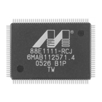
88E1111 Product Brief
Integrated 10/100/1000 Ultra Gigabit Ethernet Transceiver
Copyright © 2020 Marvell
December 2, 2020
 Loading...