AF008-02-1201
34
Number
Issue
Date
CN Number
1
2-
2
17-01-07
22933
Compiled
By:
S.Mynott
Date
Compiled:
08/08/06
MIT5XX/10XX
1
st
Used On:
SERVICE MANUAL
+3.3V_USB
TR4
BCW32
0V
TP101
IC7
24C64
1
2
3
7
4
6
5
8
A0
A1
A2
WP
Vss
SCL
SDA
Vcc
IC8
24C64
1
2
3
7
4
6
5
8
A0
A1
A2
WP
Vss
SCL
SDA
Vcc
TR5
BCF29
TP12
SCL
C18
470.00nF
25
R27
100.00K
0V
R35
10.00K
1
+3.3V_USB_uP
TP13
R29
30.00R
+3.3V_USB_uP
R30
30.00R
TP20
TP4
TP27
SDA
+1.8V
TP6
USB_Tx
TP32
+
C6
1.00uF
25.00
RESET
R32
1.00M
R31
10.00K
PL2
1
3
4
2
6
5
C21
22.00pF
50.00
22
TP29
0V
0V
+3.3V_USB
C22
22.00pF
50.00
TP17
+3.3V_USB
C19
100.00n
25
NOT FITTED
R21 10.00K
1 0.063
+
C15
10.00uF
16
TP16
C20
1.00n
50
USB Connector
R33
100.00K
TP22
TP21
USB_Tx
TP104
R22
10.00K
1
0.063
TP9
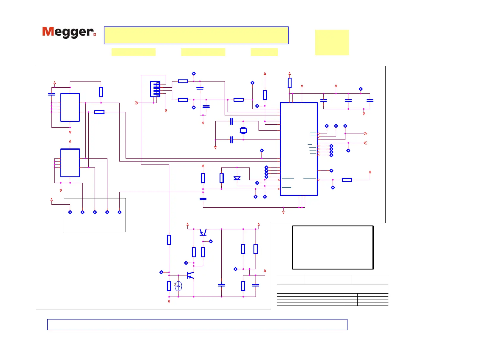
Two ways of programming - fit a preprogrammed
DIL, or fit an SO8 and program on board.
If a 5V programmer is used then the signals
should be passed through a small pcb inserted
into the programmer's zif socket. This pcb
would condition the signals to enable 3 volt
programming without damaging IC10.
R13
1.00K
1
0.063
0V
+3.3V_USB_uP
R28
4.70K
USB_Rx
TP23
TP19
USB Present
and Voltage
+3.3V_USB_uP
0V
TP100
0V
C23
22.00pF
50.00
Nonvolatile memory
holding USB enumeration
+3.3V
TP11
TP5
On board programming test pads - see notes
TP15
C16
100.00n
50.00
+5V_USB
R34
100.00K
Not Fitted (NF) List (Model 10)
D2
LL4148
TP30
R15
10.00K
1
0.063
6270-296
Interface PCB 10 & 20
A4 2 2
Tuesday, June 22, 2004
MIT5XX & 10XX
Simon Haynes 1 03-11-2004 PCD
2 03-02-05 22235
<Variant Name>
Title
Size
Document Number
Date:
Sheet of
MEGGER LIMITED
Archcliffe Road, Dover,
Kent, CT17 9EN, England
Issue Date CN No.Instrument:
Drawn By:
© MEGGER LIMITED
TP26
IC10
TUSB3410
23
9
6
7
3
5
2
26
27
28
23
24
1
4
21
20
19
17
16
15
14
13
25
32
31
30
10
11
18
8
29
22
12
RESET
DP0
DM0
VCC
PUR
SUSP
X2
X1/CLKI
GND
TEST0
TEST1
VREGEN
VDD1V8
DTR
RTS
SOUT/IR_SOUT
SIN/IR_SIN
RI/CP
DCD
DSR
CTS
VCC
P3_0
P3_1
P3_3
SDA
SCL
GND
GND
P3_4
CLKOUT
WAKEUP
Prog 5V
R20 1.50K
1
0.063
TP8
C11
100.00n
50.00
TP39
TP7
R25
3.00R
R26
30.00K
0V
TP103
+3.3V_USB
TP28
R23
15.00K
DISCHG
C17
22.00pF
50.00
22
C2, C6, C8, C9, C11, C12, C13, C15, C16, C17
C18, C19, C20, C21, C22, C23, C25
D2, D3
IC7, IC8, IC10
PL2
R1, R2, R5, R8, R9, R11, R13, R15, R17, R18,
R19, R20, R21, R22, R23, R25, R26, R27, R28
R29, R30, R31, R32, R33, R34, R35, R36, R37
R38, R41
TR1, TR2, TR3, TR4, TR5, TR6, TR7
VR1
XL1
+5V
TP31
D3
BAS16
0V
TP18
+1.8V
MHz
XL1
12.00
USB_Rx
TP10
Components fitted for Model 20 only
TP102
 Loading...