dsPIC33/PIC24 Family Reference Manual
DS30009740B-page 12 2010-2013 Microchip Technology Inc.
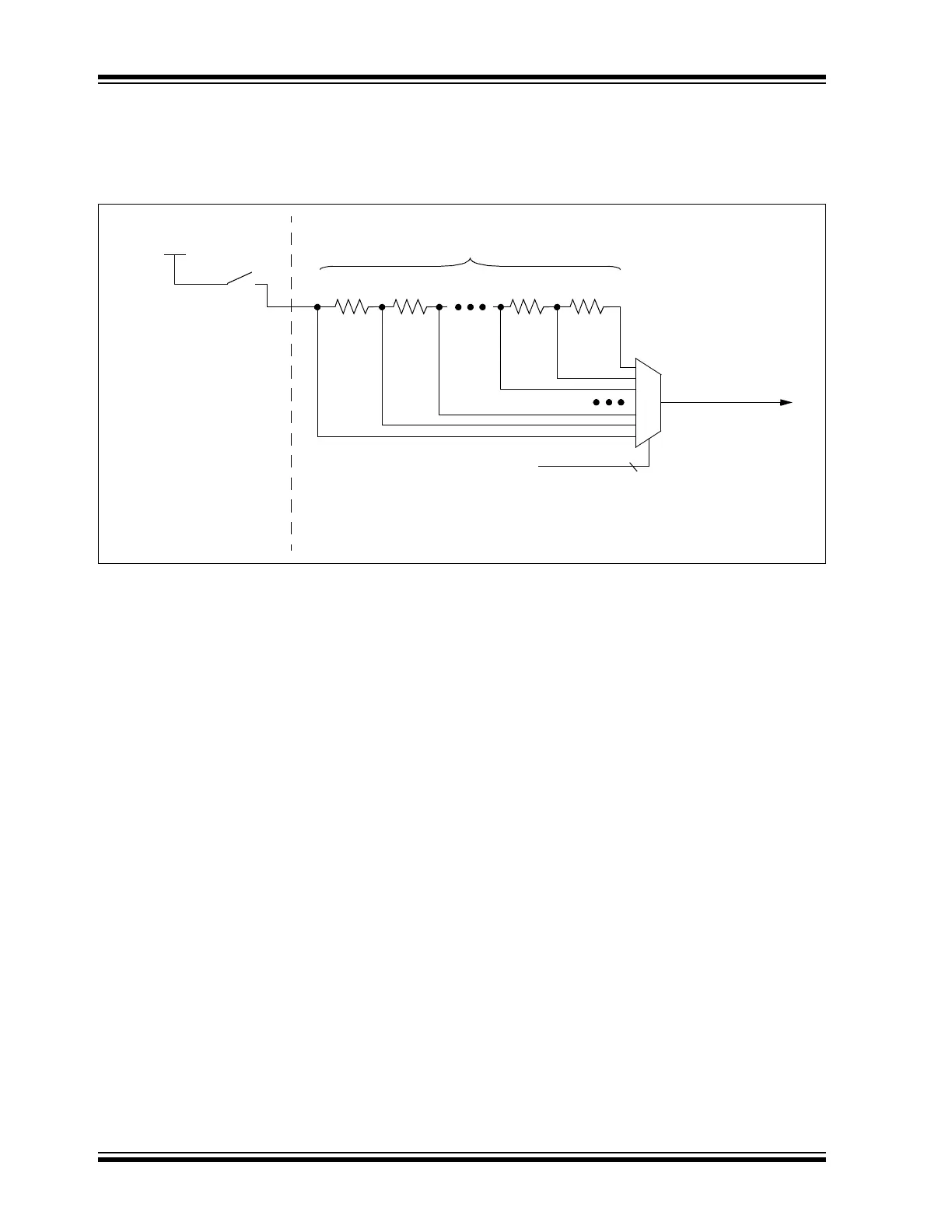
5.1.2 CONTRAST CONTROL
The LCD contrast control circuit consists of a 7-tap resistor ladder, controlled by the
LCDCST<2:0> bits (see Figure 5-3).
Figure 5-3: Internal Reference and Contrast Control Block Diagram
5.1.3 INTERNAL REFERENCE
Under firmware control, an internal reference for the LCD Bias voltages can be enabled. When
enabled, the source of this voltage can be V
DD.
When no internal reference is selected, the LCD contrast control circuit is disabled and the LCD
Bias must be provided externally. Whenever the LCD module is inactive (LCDA = 0), the internal
reference will be turned off.
5.1.4 VLCDxPE PINS
The VLCD3PE, VLCD2PE and VLCD1PE pins provide the ability for an external LCD Bias
network to be used instead of the internal ladder. Use of the VLCDxPE pins does not prevent use
of the internal ladder.
Each VLCDxPE pin has an independent control in the LCDREF register, allowing access to any
or all of the LCD Bias signals.
This architecture allows for maximum flexibility in different applications. The VLCDxPE pins could
be used to add capacitors to the internal reference ladder for increasing the drive capacity. For
applications where the internal contrast control is insufficient, the firmware can choose to enable
only the VLCD3PE pin, allowing an external contrast control circuit to use the internal reference
divider.
LCDCST<2:0>
Analog
RR RR
7 Stages
MUX
To Top of
Reference Ladder
7
0
3
VDD
Internal Reference
Contrast Control