Hardware Description
2020 Microchip Technology Inc. DS50002927A-page 33
3.2.3 Three-Phase Inverter Bridge
The three-phase motor power stage is implemented using six N-channel MOSFETs,
configured as three half-bridges. A resistor is connected across the gate and source of
each MOSFET to ensure a soft turn-off of the MOSFET when the gate signal is
disconnected. Low-ESR ceramic capacitors are provided across each half-bridge for
filtering high-frequency noise. The output of the three-phase inverter bridge is available
on connector J14.
Three half-bridge gate drivers (3 x MIC4605) are used for driving the low-side and
high-side MOSFETs of the motor control inverter. The high-side driver is powered by the
bootstrap circuit. The bootstrap circuit consists of an internal diode and an external
capacitor connected across to the gate driver HS and HB pins. The input pull-down resis-
tors are internal to the gate driver. The gate drivers are powered by a +12V supply. Even
though the HS pin is rated for negative voltage, a diode resistor clamp is provided to
clamp the negative voltage on the HS pin to prevent excessive negative voltage from
damaging the driver. Depending upon the application and amount of negative voltage on
the switch node, a different resistor and diode can be selected. For more information,
refer to the “MIC4605 Data Sheet” (DS20005853) at: www.microchip.com.
3.2.4 Current Sensing Circuits
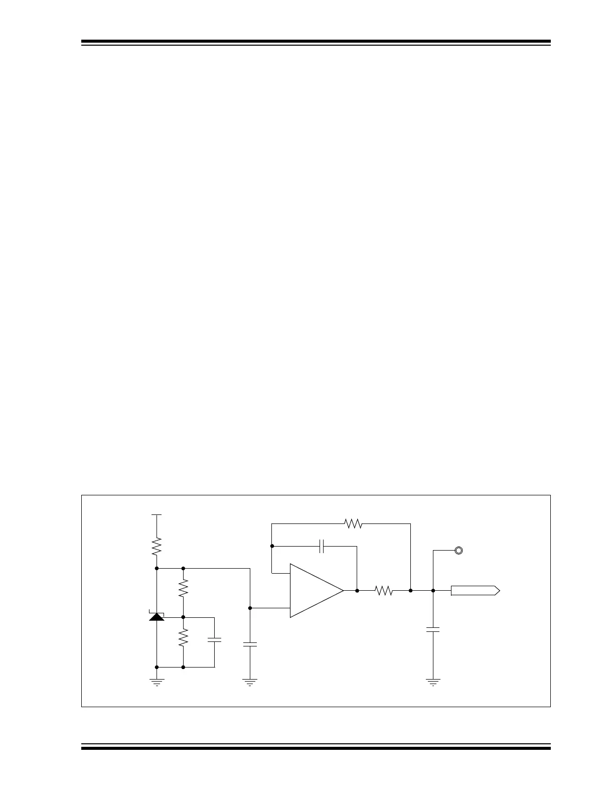
3.2.4.1 VOLTAGE REFERENCE CIRCUIT
The Reference Voltage (V
REF) is generated on the Motor Control Board; it is half the
analog supply voltage (+3.3 VA), that is, approximately +1.65V. This is used for provid-
ing a DC voltage shift on the op amp output, allowing measurement of positive and
negative current swings as a single supply amplifier is used for current amplification.
The reference circuit (see Figure 3-3) is built around one of the MCP6024 op amps
(labeled as ‘D’). The resistors, R117, R119 and R120, form the voltage divider circuit
and generate a voltage equal to half of the analog voltage (+3.3 VA). The op amp, U5D
(MCP6024-D), is used as a buffer. The resistors, R114, R118 and C70, form a compen-
sation circuit to drive capacitive loads, where C70 acts as a high-frequency feedback
path and R114 is used as a feedback path for low-frequency signals. The reference
voltage is connected to the inputs of the current sensing amplifiers providing DC bias
to amplifier outputs.
FIGURE 3-3: VOLTAGE REFERENCE CIRCUIT
+3.3 VA
R117
10k
R119
2.49k
U10
DNP
R120
7.5k
C74
DNP
C75
0.1 µF
AGND AGND AGND
R114
1k
C70
1000 pF
U5D
-D
+D
OUTD
MCP6024
R118
20R
V
REF
TP17
C72
0.1 µF
V
REF
13
12
14
1
32