2020 Microchip Technology Inc. DS50002927A-page 43
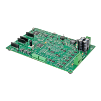
dsPIC33CK LOW-VOLTAGE
MOTOR CONTROL BOARD
USER’S GUIDE
Appendix A. Schematics and Layout
A.1 BOARD SCHEMATICS AND LAYOUT
This section provides schematics and PCB layout diagrams of the dsPIC33CK
Low-Voltage Motor Control Board. The Motor Control Board uses a four-layer FR4, 1.6
mm, Plated-Through-Hole (PTH) construction.
Ta b l e A -1 summarizes the schematics of the Motor Control Board:
TABLE A-1: SCHEMATICS
Ta b l e A -2 summarizes the layout diagrams of the Motor Control Board:
TABLE A-2: PCB LAYERS
Figure Index
Schematics
Sheet No.
Hardware Sections
Figure A-1 1 of 8 Input Power Supply Connections: +12V DC-DC Converter;
+5V DC-DC Converter; +3.3V LDO
Figure A-2 2 of 8 dsPIC33CK256MP508 Interconnections: MCLR
Reset;
ICSP™ Header; dsPIC
®
DSC Operational Amplifiers for
amplifying Bus Current and Phase Currents
Figure A-3 3 of 8 1.65V Voltage Reference Buffer: External Operational
Amplifiers for amplifying Bus Current and Phase Currents;
Potentiometer; DC Bus Voltage Sensing Circuit; Phase
Voltages Sensing Circuit; Temperature Sensing Circuits
Figure A-4 4 of 8 Motor Control Inverter: Gate Drivers; Three-Phase MOSFET
Bridge
Figure A-5 5 of 8 Click Board Sockets (A, B); LED Indications; Push Buttons;
USB to UART Converter
Figure A-6 6 of 8 Hall Sensor Interface Circuit; Quadrature Encoder Interface
Circuit
Figure A-7 7 of 8 PKOB: Microcontroller; USB Port, etc.
Figure A-8 8 of 8 PKOB: Buffers
Figure Index Description
Figure A-9 Top Layer: Top Silk and Top Copper
Figure A-10 Mid Layer -1: Copper
Figure A-11 Mid Layer -2: Copper
Figure A-12 Bottom Layer: Bottom Silk and Bottom Copper