2016-2023 Microchip Technology Inc. DS50002489G-page 9
RN4870/71
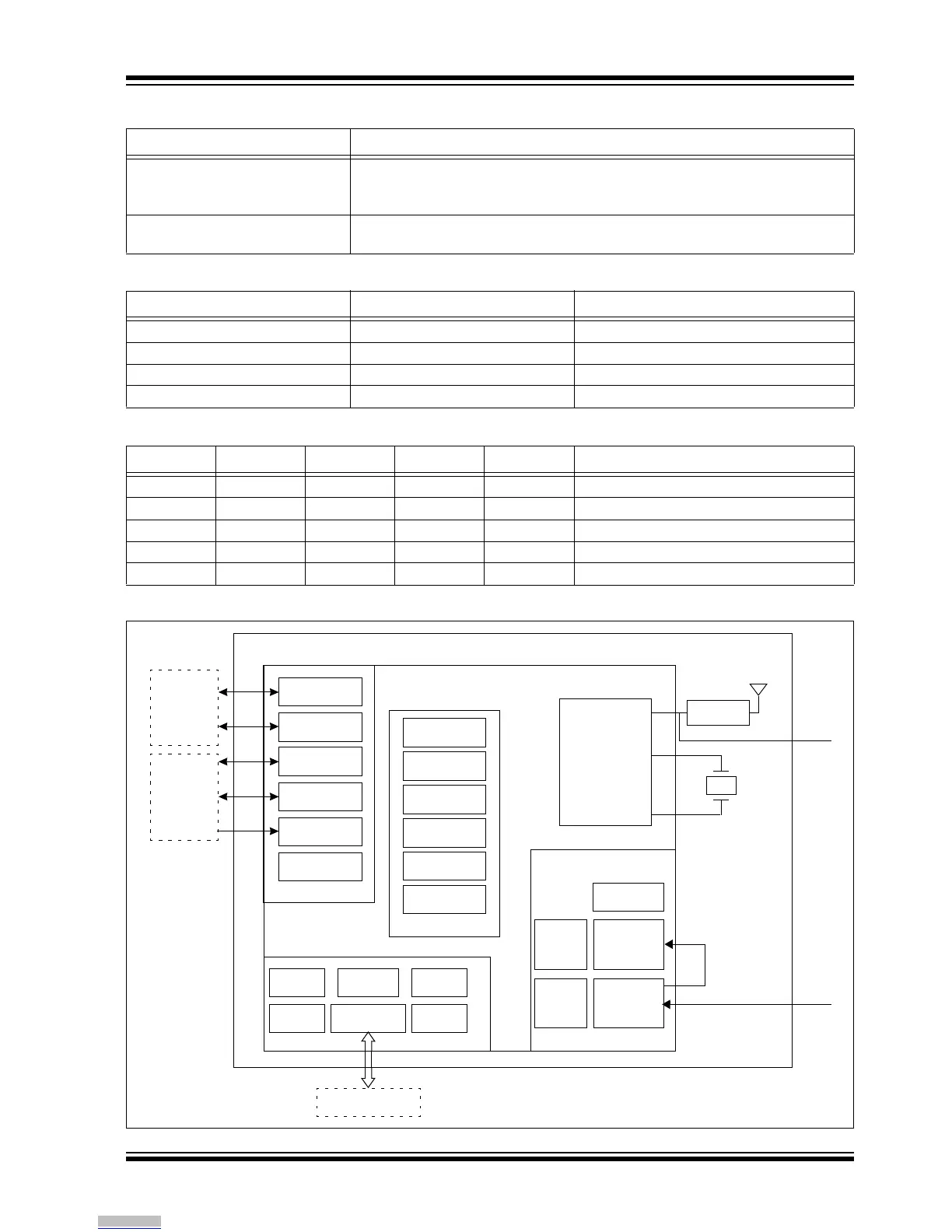
FIGURE 1-5: BLOCK DIAGRAM OF THE RN4870/71
Pairing Key When the RN4870/71 is connected to a remote device, the host MCU can use
the Pairing Key pin to force the module to disconnect the link and go back to
Standby state. The pin must be pulled down for at least 160 ms.
RF Active Indication Use this indication pin to indicate that the module is currently performing an
active transmission and receiving BLE data.
TABLE 1-5: STATUS INDICATION PINS
Status 1 Status 2 State
High High Power-on
High Low Standby state
Low Low Connection established
Low High Data session open (Transparent UART)
TABLE 1-6: TEST POINTS ON THE BOTTOM SIDE
RN4870U RN4870 RN4871U RN4871 Symbol Description
TP-1 TP-1 TP-3 TP-3 VCC_PA 1.55V RF PA LDO
TP-2 TP-2 TP-1 TP-5 CLDO_O 1.2V CLDO Output
TP-3 TP-3 TP-2 TP-2 VCC_RF 1.2V RF LDO Output
— — TP-4 TP-4 ULPC_O 1.2V ULPC LDO Output
— — TP-5 TP-1 BK_O 1.55V Buck Reg Output
TABLE 1-4: CONFIGURABLE FUNCTIONS AND DESCRIPTIONS (CONTINUED)
Function Name Description
Bluetooth
®
POR
RTC
512B
Ret-RAM
GPIO PORT
0 ~ 3
32 kHz
ROSC
LDO
MCU/GPIO/LED
Host
Controller
(Ext. MCU)
IOT
Peripheral
Device
SPI
UART
I
2
C
PWM
ADC-12b
Event
Counter
8051 (16 MHz)
32 KB ROM
24 KB SRAM
Flash 256 KB
DMA, WDT,
NMI, IRQ
AES 128
MCU
BLE
Baseband
and RF
Matching
Antenna
32 MHz
Crystal
BT_RF
PMU/MM
Tem p .
Sensor
BAT
Detect
Band Gap
LDOs
DC-DC
Converter
VBAT
Peripherals
*
Always On (AON)
*GPIO Pad on Module
RN4870/RN4871
Downloaded from Arrow.com.