2016-2023 Microchip Technology Inc. DS50002489G-page 15
RN4870/71
4.0 PHYSICAL DIMENSIONS AND
ATTRIBUTES
4.1 RN4870 Module
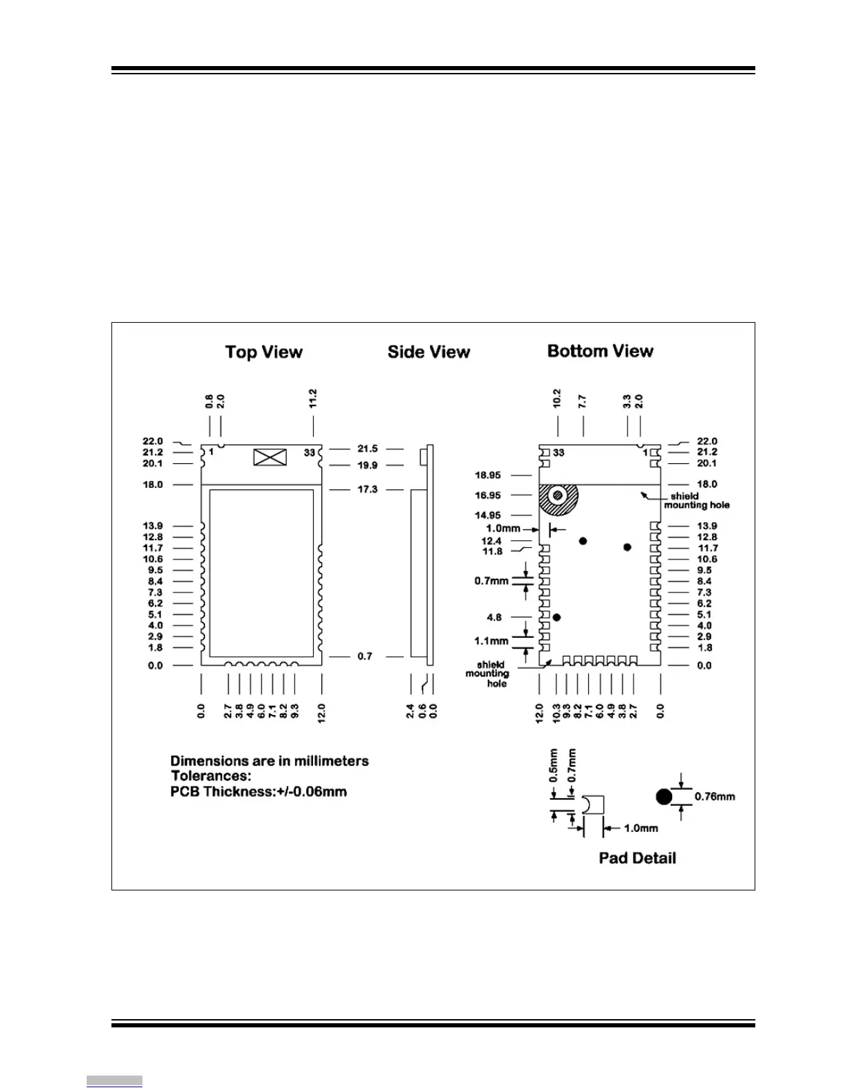
Figure 4-1 shows the physical dimensions of the RN4870
module. Figure 4-2 illustrates the recommended PCB
layout and Figure 4-3 shows the recommended
mounting details.
Ensure that there is no top copper layer near the test
pin area, indicated by the shaded keep out areas, as
shown in Figure 4-2. When laying out the host PCB, the
areas under the antenna must not contain any top,
inner layer or bottom copper, as shown in Figure 4-3. A
low-impedance ground plane ensures the best radio
performance (best range, lowest noise). Figure 4-3
also shows a minimum ground plane area to the left
and right side of the module for best antenna
performance. The ground plane can be extended
beyond the minimum recommended as required for
host PCB EMC noise reduction. For best range
performance, keep all external metal at least 30 mm
away from the ceramic chip antenna.
FIGURE 4-1: RN4870 MODULE DIMENSIONS
Downloaded from Arrow.com.