Description of Test Design
UG0048 User Guide Revision 5.1 15
5 Description of Test Design
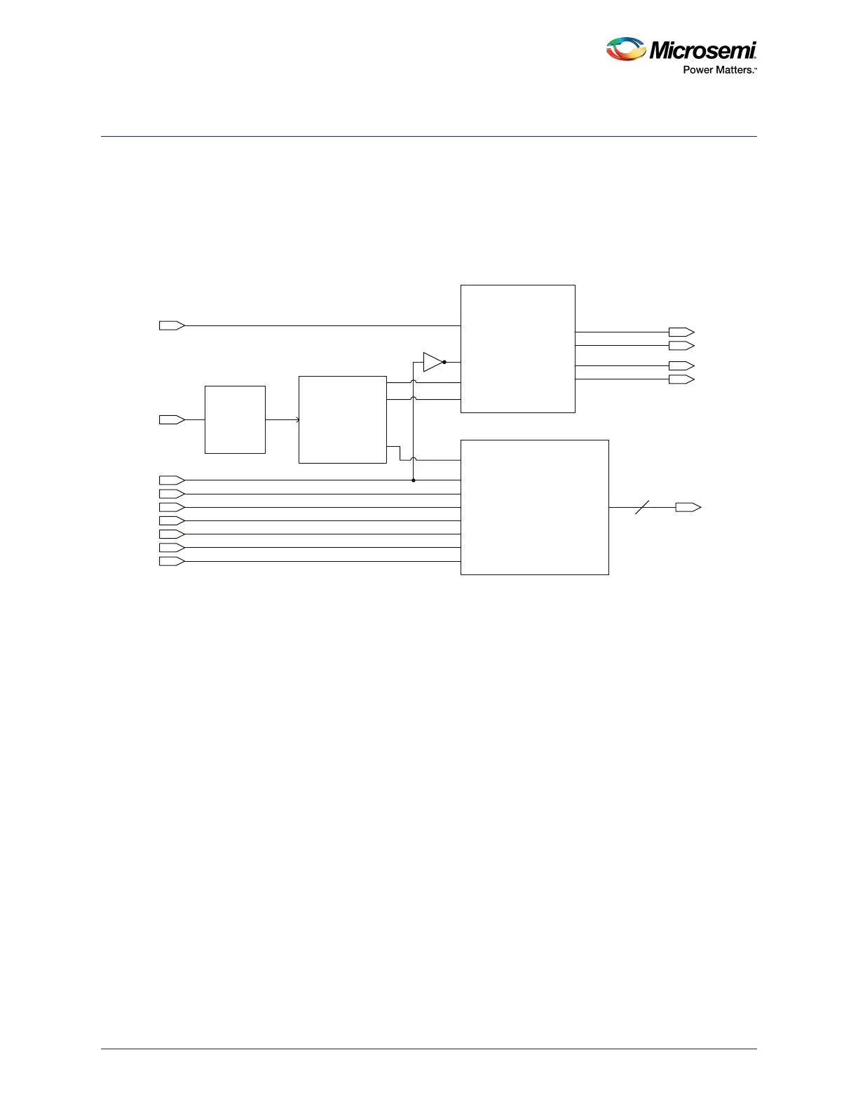
The description of the test design is provided with the Starter Kit. This design contains a data generator
block for LEDs, PLL for clock generation, and an OLED display driver block. A block diagram of the
design is shown in the following figure.
Note: The latest version of the board A3PE-STARTER-KIT-2 REV B does not have OLED display. For more
information, see the CN1418A: Addendum A: Designing without OLED Display on Kits.
Figure 3 • Design Block Diagram
The on-chip PLL takes a 40 MHz oscillator clock as reference input and generates 2.5 MHz clock for the
design. The data generator (Data_Block) generates an eight-bit up-down counter and eight-bit flashing
signal. The data generator output is displayed on the ProASIC3/E starter kit board LEDs. By default, an
eight-bit flashing signal is displayed on the LEDs. The LEDs flashing direction can be changed by
pressing SW4. Switch the data using the SW6 signal. The counter has synchronous load and an
asynchronous clear. The counter can be loaded with the hex switches data by pressing SW3. Press and
hold SW2 for down counting.
HexA[3:0]
OLED _CLK
CLK
Direction
UpDown
Aclr
sload
Data_select
HexB[3:0]
pacer_rst
scl
sda
Power_up_del
start
resetn
OLED _init
DATA_LED[7:0]
Data_Block
OLED_driver
Counter [19:0]
PLL
cnt[19]
cnt[18]
cnt[1]
GLACLKA
40MHz
2.5 MHz
SW1
SW2
LED[7:0]
SW6
SW5
SW4
SW3
HexA[3:0]
HexB[3:0]
SDA
SCL
Pacer_rst
OLED_init