LVDS Signal Evaluation
UG0048 User Guide Revision 5.1 17
6 LVDS Signal Evaluation
This section explains the test setup and design for the LVDS signal evaluation. It reports the
measurements performed on the board, and at the end, makes recommendations to increase the LVDS
signal quality in order to meet the performance criteria.
6.1 Hardware Test Setup
The test setup uses a ProASIC3 Development Kit containing an A3PE600-PQ208 engineering sample.
LVDS loop-back is closed using various lengths of CAT-5E cables (1-, 3-, and 6-foot). The measurements
are taken using a 1159A-1 GHz Agilent differential probe.
6.2 Design Test Setup
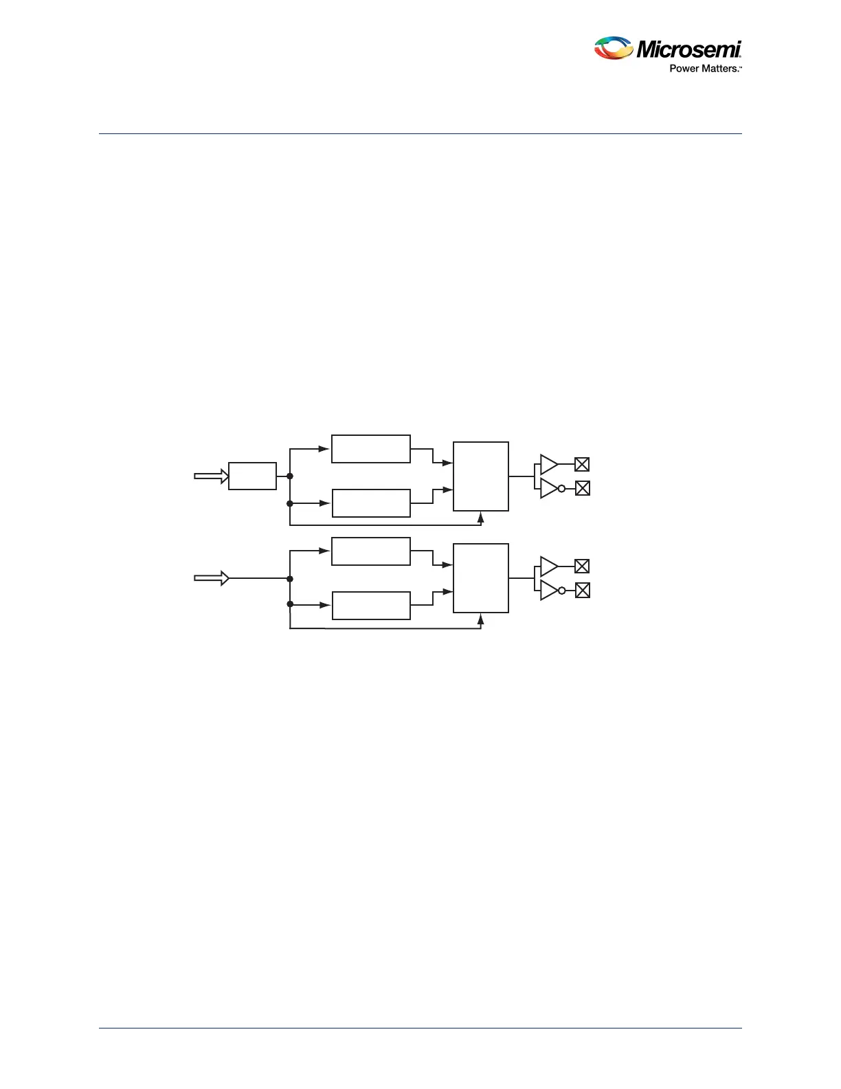
The following figure shows the block diagram of the transmitter section of the test design programmed
inside the ProASIC3 FPGA. The design contains two similar channels of data. Channel A is driven by a
PLL to achieve high data rates, and Channel B uses an external clock in the event that slow data rates
are needed for test or debugging purposes.
Figure 5 • TX Portion of Test Design
Each channel uses an LFSR to generate a pseudo-random data stream. The data stream is entered in
DDR registers to achieve higher data rates from relatively slower clocks (e.g., 300 Mbps data rate from
150 MHz clock). The output of the DDR registers is sent out using the LVDS I/O standard. The output
data is looped back and received by the FPGA using LVDS receivers.
PLL
clk
out
clk
LFSR_2
out
DDR-REG
Qf
Qr
Clk
Dout
LFSR_1
clk
out
clk
LFSR_2
out
DDR-REG
Qf
Qr
Clk
Dout
CLK_1
LK_2
Channel
Channel