473
APPENDICES
A
Appendix 3 CPU Module Processing Time
Appendix 3.2 Time required for each processing included in scan time
(b) Error clear
The following processing time is required to clear continuation errors stored in SD50 on the rising edge of
SM50 (Error reset).
(c) Error clear by types
The following processing time is required to clear continuation errors by types.
(6) Device data latch processing time
When the latch range is set in the Device tab of the PLC parameter dialog box
*1 *2 *3
, the processing time listed in
the following tables is required. Each N1, N2, and N3 in the table indicates the following.
• N1: Number of devices specified to be latched (Count the latch range (1) and the latch range (2) as different
devices.)
• N2: Number of bit device points specified to be latched
• N3: Number of word device points specified to be latched
(a) When the latch interval is set to "Each Scan"
The processing time listed in the following table is required.
*1 When setting the latch range of the timer (T), retentive timer (ST), and counter (C), one point for word device and two
points for bit device are occupied per point.
*2 The case where the points are set for the latch relay (L) is included.
*3 The scan time will not increase if the latch range is set for the file register (ZR), extended data register (D), or extended
link register (W).
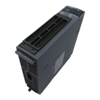
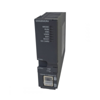
CPU module
Processing time in END processing
When the error is cleared
(the one detected by the
annunciator)
When the error is cleared
Q00UJCPU, Q00UCPU, Q01UCPU 0.185ms 0.180ms
Q02UCPU 0.180ms 0.175ms
Q03UD(E)CPU 0.068ms 0.062ms
Q04UD(E)HCPU, Q06UD(E)HCPU, Q10UD(E)HCPU, Q13UD(E)HCPU,
Q20UD(E)HCPU, Q26UD(E)HCPU, Q50UDEHCPU, Q100UDEHCPU
0.065ms 0.062ms
Q03UDVCPU, Q04UDVCPU, Q06UDVCPU, Q13UDVCPU,
Q26UDVCPU
0.03ms 0.026ms
CPU module
Processing time in END processing
When the error is cleared
(the one detected by the
annunciator)
When the error is cleared
Q03UDVCPU, Q04UDVCPU, Q06UDVCPU, Q13UDVCPU,
Q26UDVCPU
0.04ms 0.036ms
CPU module Processing time
Q00UJCPU, Q00UCPU, Q01UCPU (4.4 × N1) + (0.12 × (N2 16 + N3))µs
Q02UCPU (4.0 × N1) + (0.12 × (N2 16 + N3))µs
Q03UD(E)CPU (3.0 × N1) + (0.12 × (N2 16 + N3))µs
Q03UDVCPU (1.0 × N1) + (0.085 × (N2 16 + N3)) + 1.2µs
Q04UD(E)HCPU, Q06UD(E)HCPU, Q10UD(E)HCPU, Q13UD(E)HCPU,
Q20UD(E)HCPU, Q26UD(E)HCPU, Q50UDEHCPU, Q100UDEHCPU
(3.0 × N1) + (0.05 × (N2 16 + N3))µs
Q04UDVCPU, Q06UDVCPU, Q13UDVCPU, Q26UDVCPU (1.0 × N1) + (0.045 × (N2 16 + N3)) + 1.2µs
 Loading...