September 5, 2008 6881076C25-E
4-24 Troubleshooting Procedures: Power Amplifier Procedures
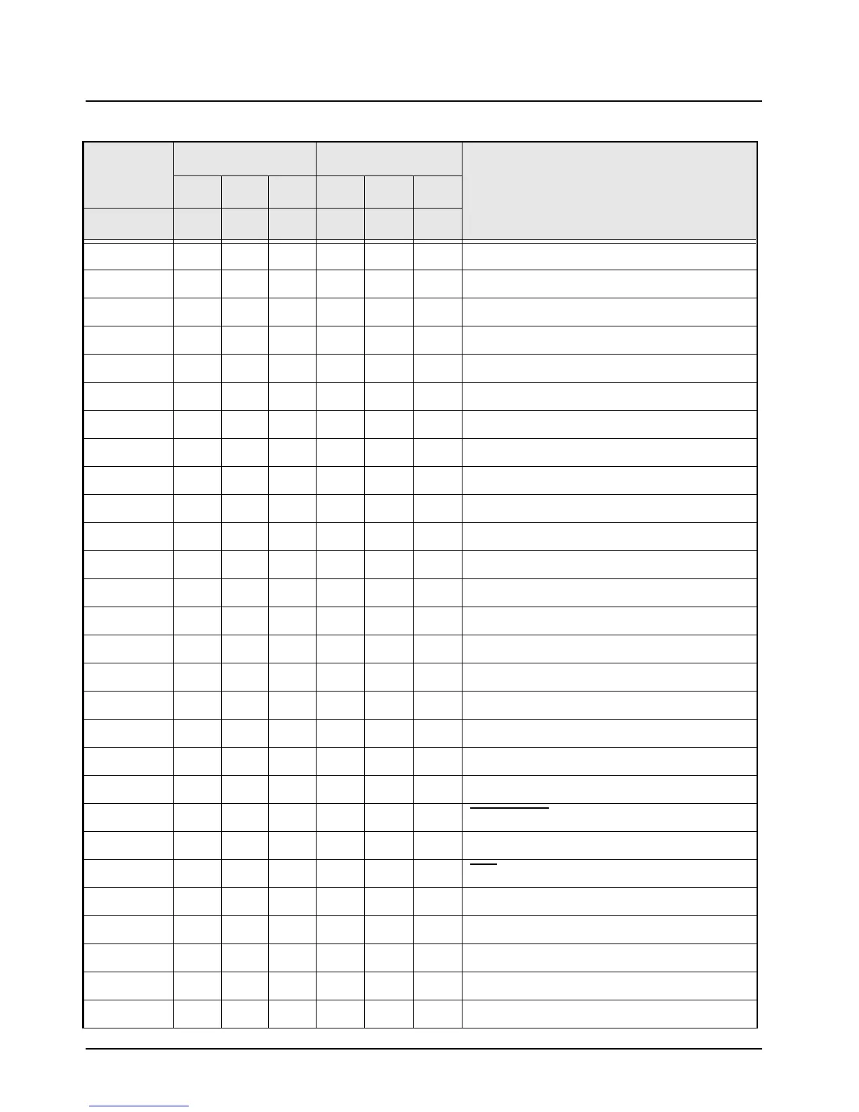
13 0 0 1.2 6.0
Thermister Buffer in
14 5.0 5.0
5-V Sense Input (follows pin 20 ±0.1 V)
15 4.9 5.0 5.7 4.9 5.0 5.7
5-V Current Limit (limits at 5.7 V)
16 5.0 5.7 6.4 5.0 5.7 6.4
5-V Series Pass Drive (6.4 at max current)
17 9.5 9.6 9.9 9.5 9.6 9.9
9.6-V Sense Input
18 7 7
5-V Reg. Compensation Capacitor
19 5.7 5.7
N.C.
20 4.9 5.0 5.1 4.9 5.0 5.1
5-V Reference Input (UNSW5V)
21 1.2 1.2
9.6-V Reg. Compensation Capacitor
22 0 0
N.C.
23 0.9 9.6 1.2 9.6
9.6-V Series Pass Drive
24 2.9 3.3
Regulator Enable/Compensation
25 ––––––
9.6-V Programming (N.C.)
26 0 0
N.C.
27 13.6 13.6
N.C.
28 ––––––
9.6-V Programming (N.C.)
29 ––––––
9.6-V Programming (N.C.)
30 ––––––
9.6-V Programming (N.C.)
31 000000
Ground
32 10.8 13.6 16.5 10.0 13.0 16.0
Decoupled A+
33 4.0 5.0 0 0.2
TX PA Enable (from U520–25)
34 0 1.3
Control AMP one-shot
35 0 0
Lock (5 V of Synth Out of Lock)
36 0 0.8
Control AMP one-shot
37 10.8 13.6 16.3 10.0 13.0 16.0
A+ (Current Sense +)
38 10.8 13.6 16.3 10.0 13.0 16.0
Current Sense - Voltage Delta 150 mV
39 0 9.2 9.4 9.8
Keyed 9.4-V in
40 1.5 3.0 4.5 1.5 3.0 4.5
Current Limit D-A (max current at 4.5 V)
Table 4-8. Power Control DC Voltage Chart (Continued)
LOCATION
RX MODE TX MODE
COMMENTS
LOW TYP HI LOW TYP HI
J1
 Loading...