The RF PA module is a multi-stage amplifier, which
has the required gain to produce an output level of sev-
eral watts. Some harmonic filtering is accomplished in
the RF PA.
Power control is achieved by using the coupler
detector to feed back a portion of the PA output to the
ALC circuit. This ALC circuit increases or decreases the
overall PA gain as appropriate. Another function of the
detector is to provide a signal when the VSWR exceeds
the threshold level. This signal, combined with the
forward detected power, is used to reduce the PA output
power, thus protecting the PA under high VSWR
conditions.
IV. 800/900MHz TRANSCEIVER BOARD
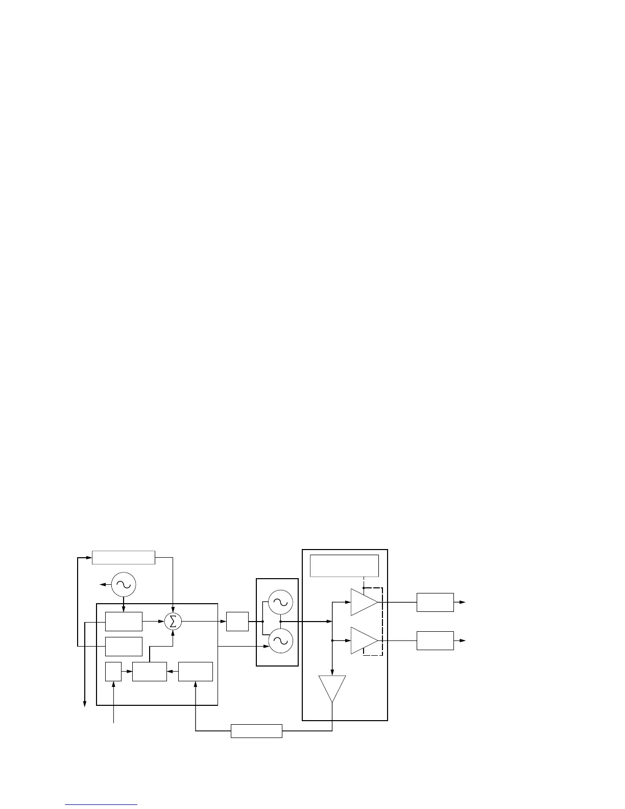
A. Frequency Generation Unit (See Figure 5)
The frequency generation unit (FGU) consists of the
following major sections: the high stability reference
oscillator (U203), fractional-N synthesizer (U204), VCO
buffer IC (U201), and VCO (U205). The VCO provides
the carrier frequency for the transmitter (TX OUT), and
provides the local oscillator (LO) injection signal for the
receiver mixer buffer (RX OUT). The phase lock loop
(PLL) circuit is provided by the fractional-N synthesizer
IC.
The output of the VCO is amplified by the prescaler
buffer, routed through a low-pass filter, and applied to
the prescaler dividers of the synthesizer. The divide
ratios are determined from information stored in memory
that is bussed to the synthesizer via the microprocessor.
The microprocessor extracts data for the division ratio
as determined by the channel-select switch. The resul-
tant VCO buffer signal is applied to a comparator in the
synthesizer. The synthesizer comparator also receives a
reference frequency via a reference divider input from
the 16.8 MHz temperature-compensated reference
oscillator. If the two frequencies differ, the synthesizer
generates a control (error) voltage which causes the
VCO to change frequency.
Modulation of the carrier is achieved by using a 2-
port modulation technique. The deviation of the low
frequency tone, such as DPL/TPL, is achieved by inject-
ing the signal to an analog/digital circuit in the
synthesizer. The resultant digitized signal is then modu-
lated by the fractional N-divider, thus generating the
required deviation. The deviation of the high frequency
tone is achieved by modulating the modulation varactor
on the VCO. In order to cover a very wide bandwidth,
the VCO control voltage is stepped up by using a posi-
tive multiplier circuit. A 13-volt supply powers the phase
detector circuitry. The VCO signal is amplified by the
integrated buffer amplifier of the VCO buffer. The two
output signals, receiver first LO injection and transmitter
carrier frequency, are filtered and then routed to the
mixer/buffer (U2) and the RF PA (U105), respectively.
B. Antenna Switch
The function of the antenna switch is to route the
transmitter power to the antenna during the transmit
mode, or route the RF from the antenna, to the receiver
front end during the receive mode.
C. Receiver Front End (See Figure 6)
The RF signal from the antenna is coupled to the
first bandpass filter through the antenna switch. The out-
put of the bandpass filter is then applied to a wideband
RF amplifier IC (RF AMP). The bandpass filter is a wide-
band stripline filter, which is pretuned for the frequency
band. After amplification, the RF signal is further filtered
by a second fixed-tuned stripline filter to improve the
spurious rejection.
The filtered RF signal is then applied to the RF input
of a broadband mixer IC, U2. An injection signal (FIRST
LO) supplied by the FGU, is applied to the second input
of the mixer stage. The resulting difference frequency of
73.35MHz is the first IF frequency. The first IF frequency
is then filtered by a 2-pole crystal filter, FL1, to remove
unwanted mixer products and routed to the IF IC, U3
6
 Loading...


