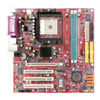
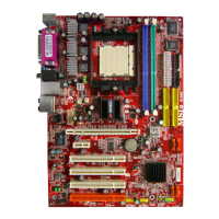
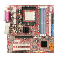
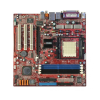
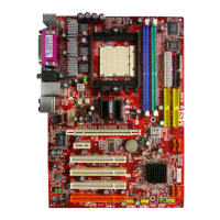
MS-7248 Mainboard
2-16
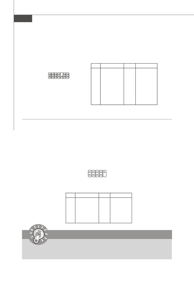
JLPC1 Pin Definition
PIN SIGNAL PIN SIGNAL
1 LCLK 2 Key (no pin)
3 LRST# 4 VCC3
5 LAD0 6 FID0_LRST
7 LAD1 8 VCC5
9 LAD2 10 Key (no pin)
11 LAD3 12 GND
13 LFRAME# 14 GND
FWH/LPC Debugging Pin Header: JLPC1
The pin header is for internal debugging only.
JLPC1
13
14
2
1
Front USB Connectors: JUSB1, JUSB2
The mainboard provides two USB 2.0 pinheaders (optional USB 2.0 bracket available)
that are compliant with Intel
®
I/O Connectivity Design Guide. USB 2.0 technology
increases data transfer rate up to a maximum throughput of 480Mbps, which is 40
times faster than USB 1.1, and is ideal for connecting high-speed USB interface
peripherals such as USB HDD, digital cameras, MP3 players, printers, mo-
dems and the like.
1
2
9
10
JUSB1/2
PIN SIGNAL PIN SIGNAL
1 VCC 2 VCC
3 USB0- 4 USB1-
5 USB0+ 6 USB1+
7 GND 8 GND
9 Key (no pin) 10 USBOC
Pin Definition
Important
Note that the pins of VCC and GND must be connected correctly to avoid
possible damage.
 Loading...