NI USB-6001/6002/6003 User Guide | © National Instruments | 19
The main blocks of the AO circuitry are as follows:
• Protection—The protection circuit prevents damage of the buffers in case of a short circuit
or an overvoltage condition.
• Buffer—The buffer amplifies the analog signal to the ±10 V range and ensures the driving
capability for the external load.
• DAC 0 and DAC 1—The Digital to Analog Converters (DAC) convert the digital signals
into low-level analog signals.
• AO FIFO—The AO FIFO (first-in-first out) ensures that data is transferred to the DACs
in a timely manner without being affected by USB latencies.
• DAC Control—The DAC control sets the DAC data rate and the startup condition, which
could be triggered by PFI 0 or PFI 1.
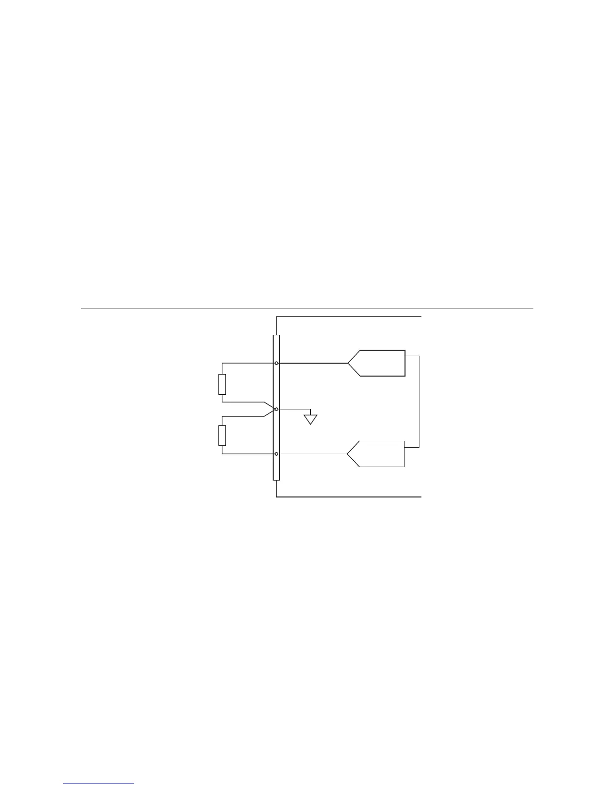
Connecting Analog Output Signals
The analog output signals are referenced to AO GND. Connect the loads between AO 0 or AO 1
and AO GND.
Figure 12. Connecting the Analog Ouput Loads
Power-On State
The AO exhibits a short glitch when the device is powered on and when the NI DAQ dev ice
exits suspend mode. After power-up, the AO is reset to 0 V.
AO Range
The AO range is ± 10 V.
 Loading...