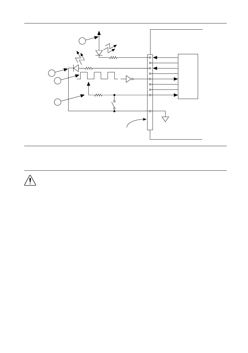
Figure 7. Example of Connecting a Load
+5 V
LED
Switch
I/O Connector
GND
P0.0
P0.1
P0.2
P0.3
P0.4
P0.5
P0.6
P0.7
+5 V
LED
1
2
3
4
TTL Signal
1. P0.0 configured as an open collector digital output
driving an LED
2. P0.2 configured as a active drive digital output
driving an LED
3. P0.4 configured as a digital input receiving a TTL
signal from a gated inverter
4. P0.7 configured as a digital input receiving a 0 V
or 5 V signal from a switch
Caution Exceeding the maximum input voltage ratings or maximum output ratings
listed in the device specifications can damage the DAQ device and the computer.
National Instruments is not liable for any damage resulting from such signal
connections.
I/O Protection
Each DIO signal is protected against overvoltage, undervoltage, and overcurrent conditions, as
well as ESD events. However, you should avoid these fault conditions by using the following
guidelines:
• If you configure a DIO line as an output, do not connect it to any external signal source,
ground signal, or power supply.
• If you configure a DIO line as an output, understand the current requirements of the load
connected to these signals. Do not exceed the specified current output limits of the DAQ
device.
• If you configure a DIO line as an input, do not drive the line with voltages outside of its
normal operating range.
• Treat the DAQ device as you would treat any static-sensitive device. Always properly
ground yourself and the equipment when handling the DAQ device or connecting to it.
10 | ni.com | NI USB-6501 User Guide
 Loading...