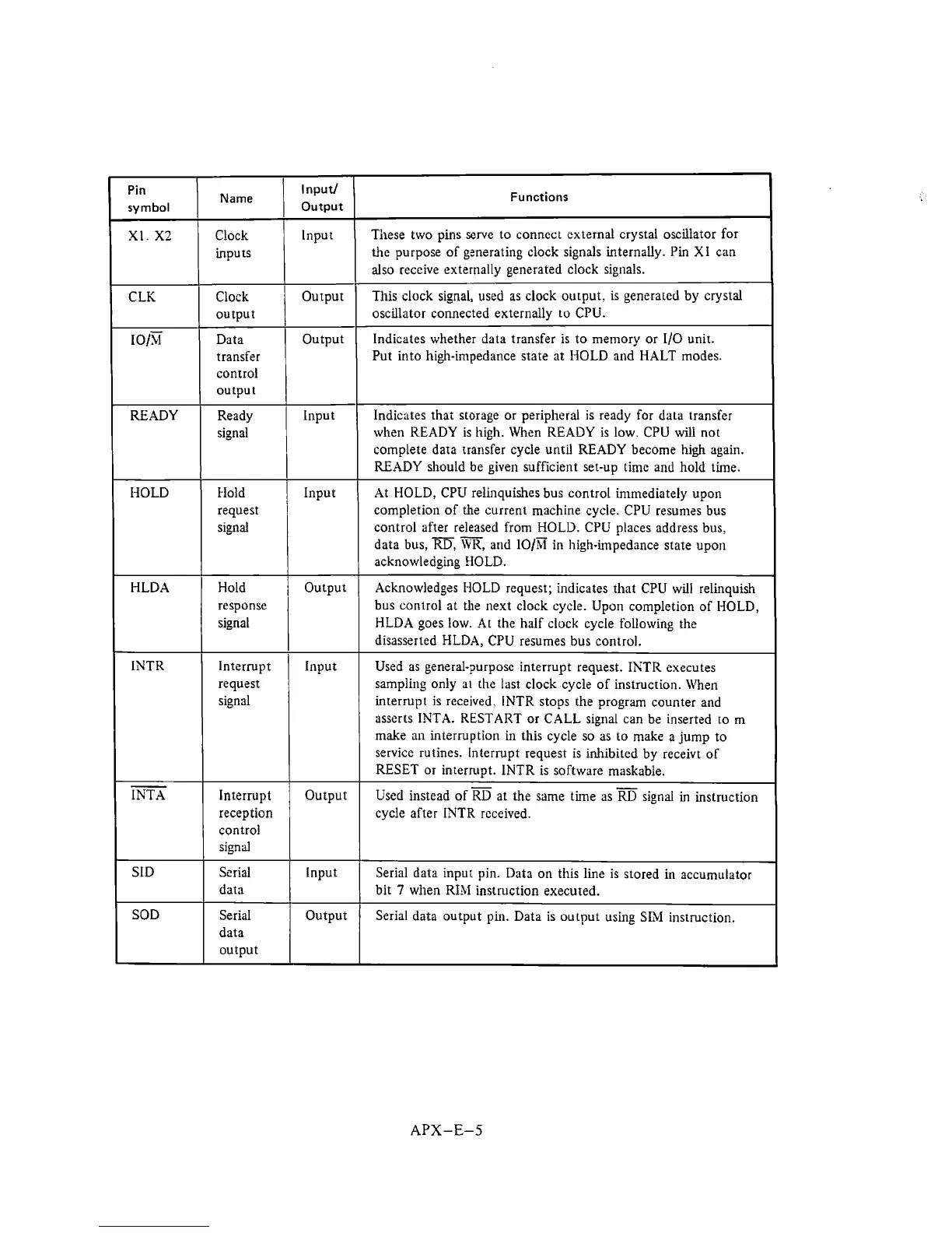
Functions
These two pins serve to connect external crystal oscillator for
the purpose of
g2nerating clock signals internally. Pin XI can
also receive externally generated clock signals.
This clock signal, used as clock output, is generated by crystal
oscillator connected externally to
CPU.
Indicates whether data transfer is to memory or 110 unit.
Put into high-impedance state at HOLD
and HALT modes.
Indicates that storage or peripheral is ready for
daii transfer
when READY is high.
When READY is low. CPU will not
complete data transfer cycle until READY become
high
again.
READY
should be given sufficient set-up time and hold time.
At MOLD, CPU relinquishes bus control
immediately upon
completio~l of the current machine cycle. CPU resumes bus
control after released from HOLD. CPU places address bus,
--
data bus,
RD,
\VK, and 10/B
in
high-impedance state upon
acknowledging HOLD.
Acknowledges MOLD request; indicates that CPU will relinquish
bus control at
the next clock cycle. Upon completion of I-IOLD,
HLDA goes low.
At
the half clock cycle following the
disasserted HLDA, CPU resumes bus control.
Used as general-purpose interrupt request.
IXTK executes
sampling only a1 thc last clock cycle of instruction. Wen
interrupt is received, INTR stops the program counter and
asserrs INTA. KESTART or CALL signal can be inserted to m
make
an
interruption in this cycle so as to make a jump to
service rutines. interrupt request is inhibited by receivt of
RESET or interrupt.
INTR is software maskable.
Used instead of
at the same time as
signal
in
instruction
cycle after INTR received.
Serial data
input pin. Data on this line is stored
in
accumulator
bit
7
when
RIM
instruction executed.
Serial data output pin. Data is output using
SM
instructio~l.
Pin
symbol
XI. X2
CLK
IO/~
READY
I-IOLD
HLD A
INTI<
-
INTA
SID
SOD
Input/
Name
I
Output
Clock
inputs
Input
Clock Output
output
I
Data Output
transfer
control
output
Ready Input
signal
Hold Input
request
signal
Hold Output
response
signal
Interrupt
Input
request
signal
Interrupt Output
reception
control
signal
Serial
I
Input
data
Serial Output
data
output